NLAS4685
features guaranteed Break Before Make switching, assuring the switches never short the driver.
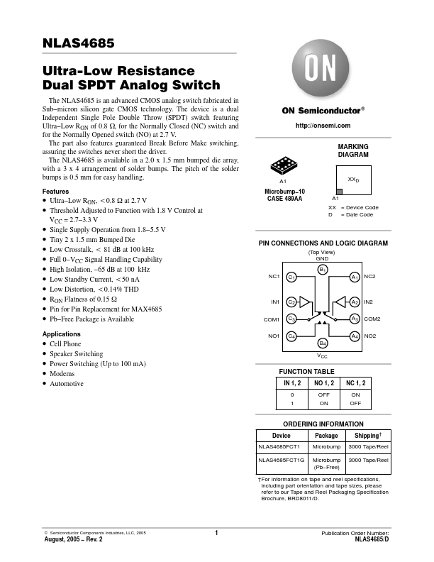
The NLAS4685 is available in a 2.0 x 1.5 mm bumped die array, with a 3 x 4 arrangement of solder bumps. The pitch of the solder bumps is 0.5 mm for easy handling.
Features
- Ultra- Low RON, t0.8 W at 2.7 V
- Threshold Adjusted to Function with 1.8 V Control at
VCC = 2.7- 3.3 V
- Single Supply Operation from 1.8- 5.5 V
- Tiny 2 x 1.5 mm Bumped Die
- Low Crosstalk, t 81 d B at 100 k Hz
- Full 0- VCC Signal Handling Capability
- High Isolation,
- 65 d B at 100 k Hz
- Low Standby Current, t50 n A
- Low Distortion, t0.14% THD
- RON Flatness of 0.15 W
- Pin for Pin Replacement for MAX4685
- Pb- Free Package is Available
Applications
- Cell Phone
- Speaker Switching
- Power Switching (Up to 100 m A)
- Modems
- Automotive http://onsemi.
MARKING DIAGRAM
A1
Microbump- 10 CASE 489AA
A1 XX = Device Code D = Date Code
PIN CONNECTIONS AND LOGIC DIAGRAM
(Top View) GND
B1
NC1 C1
A1 NC2
IN1 C2
A2 IN2
1...