Datasheet Details
| Part number | NB7L216 |
|---|---|
| Manufacturer | ON Semiconductor |
| File Size | 290.24 KB |
| Description | High Gain Receiver/Buffer/Translator |
| Datasheet |
 NB7L216 Datasheet NB7L216 Datasheet
|
|
|
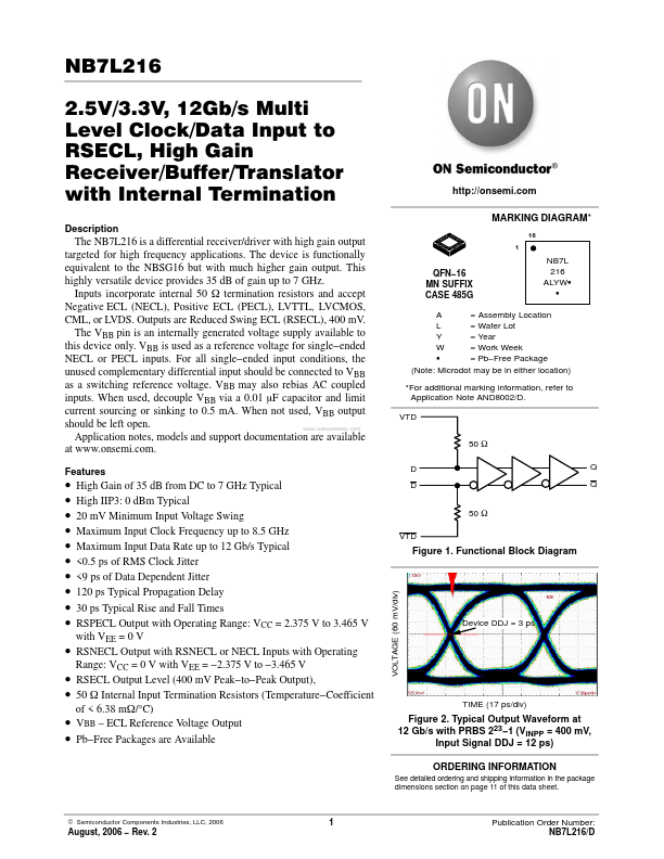
The NB7L216 is a differential receiver/driver with high gain output targeted for high frequency applications.
The device is functionally equivalent to the NBSG16 but with much higher gain output.
| Part number | NB7L216 |
|---|---|
| Manufacturer | ON Semiconductor |
| File Size | 290.24 KB |
| Description | High Gain Receiver/Buffer/Translator |
| Datasheet |
NB7L216 Datasheet
|
|
|
|