Datasheet Details
| Part number | NB7L1008 |
|---|---|
| Manufacturer | ON Semiconductor |
| File Size | 179.81 KB |
| Description | 2.5V / 3.3V 1:8 LVPECL Fanout Buffer |
| Datasheet |
 NB7L1008 Datasheet NB7L1008 Datasheet
|
|
|
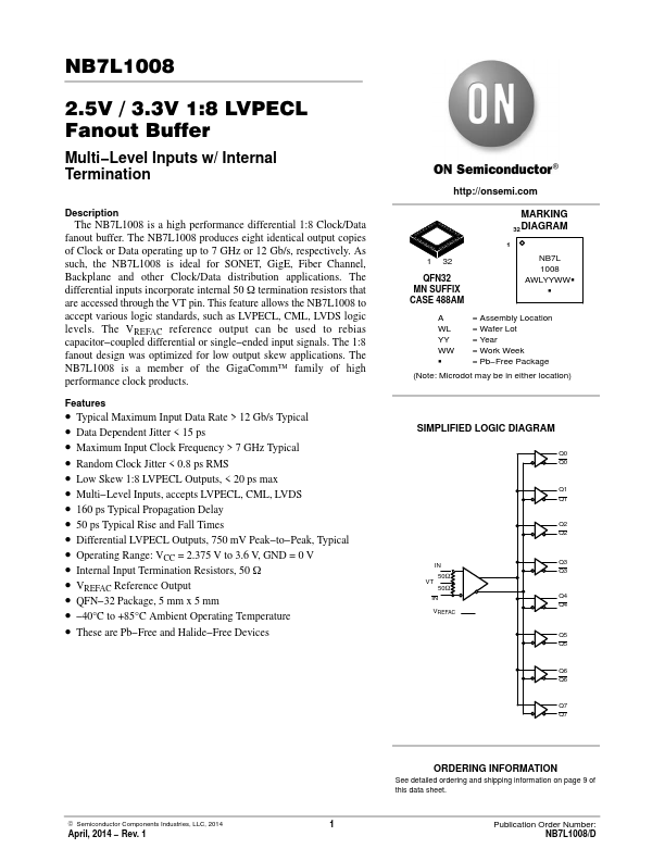
fanout buffer.
The NB7L1008 produces eight identical output copies of Clock or Data operating up to 7 GHz or 12 Gb/s, respectively.
| Part number | NB7L1008 |
|---|---|
| Manufacturer | ON Semiconductor |
| File Size | 179.81 KB |
| Description | 2.5V / 3.3V 1:8 LVPECL Fanout Buffer |
| Datasheet |
NB7L1008 Datasheet
|
|
|
|