Click to expand full text
www.DataSheet4U.com
NB2308A 3.3 V Zero Delay Clock Buffer
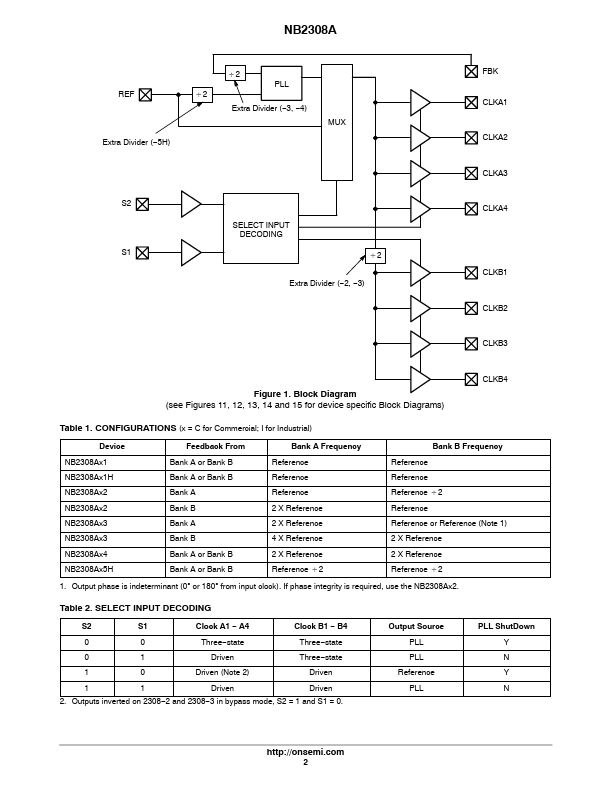
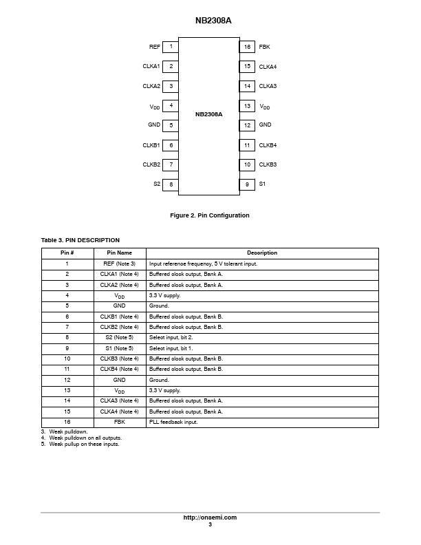
The NB2308A is a versatile, 3.3 V zero delay buffer designed to distribute high−speed clocks. It is available in a 16 pin package. The part has an on−chip PLL which locks to an input clock presented on the REF pin. The PLL feedback is required to be driven to FBK pin, and can be obtained from one of the outputs. The input−to−output propagation delay is guaranteed to be less than 250 ps, and the output−to−output skew is guaranteed to be less than 200 ps. The NB2308A has two banks of four outputs each, which can be controlled by the select inputs as shown in the Select Input Decoding Table. If all the output clocks are not required, Bank B can be three−stated.
 NB2308A Datasheet