Datasheet4U Logo Datasheet4U.com

NB2304A - Zero Delay Clock Buffer

Description

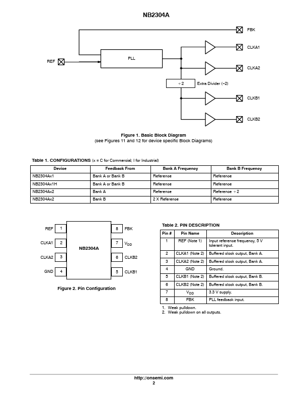
Pin # 1 2 3 4 5 Pin Name REF (Note 1) CLKA1 (Note 2) CLKA2 (Note 2) GND CLKB1 (Note 2) CLKB2 (Note 2) VDD FBK Description Input reference frequency, 5 V tolerant input.

Buffered clock output, Bank A.

Buffered clock output, Bank A.

Features

  • http://onsemi. com.

📥 Download Datasheet

Datasheet preview – NB2304A

Datasheet Details

Part number NB2304A
Manufacturer Onsemi
File Size 151.32 KB
Description Zero Delay Clock Buffer
Datasheet download datasheet NB2304A Datasheet
Additional preview pages of the NB2304A datasheet.
Other Datasheets by ON Semiconductor

Full PDF Text Transcription

Click to expand full text
www.DataSheet4U.com NB2304A 3.3 V Zero Delay Clock Buffer The NB2304A is a versatile, 3.3 V zero delay buffer designed to distribute high−speed clocks in PC, workstation, datacom, telecom and other high−performance applications. It is available in an 8 pin package. The part has an on−chip PLL which locks to an input clock presented on the REF pin. The PLL feedback is required to be driven to FBK pin, and can be obtained from one of the outputs. The input−to−output propagation delay is guaranteed to be less than 250 ps, and the output−to−output skew is guaranteed to be less than 200 ps. The NB2304A has two Banks of two outputs each. Multiple NB2304A devices can accept the same input clock and distribute it.
Published: |