Full PDF Text Transcription for MC74VHCT08A (Reference)
Note: Below is a high-fidelity text extraction (approx. 800 characters) for
MC74VHCT08A. For precise diagrams, and layout, please refer to the original PDF.
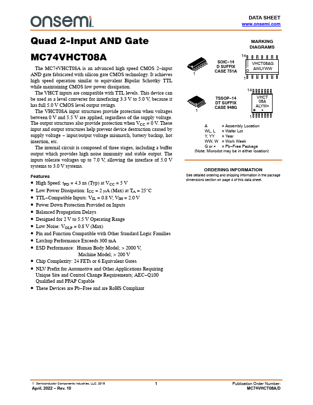
Quad 2-Input AND Gate MC74VHCT08A The MC74VHCT08A is an advanced high speed CMOS 2−input AND gate fabricated with silicon gate CMOS technology. It achieves high speed ope...
View more extracted text
bricated with silicon gate CMOS technology. It achieves high speed operation similar to equivalent Bipolar Schottky TTL while maintaining CMOS low power dissipation. The VHCT inputs are compatible with TTL levels. This device can be used as a level converter for interfacing 3.3 V to 5.0 V, because it has full 5.0 V CMOS level output swings. The VHCT08A input structures provide protection when voltages between 0 V and 5.5 V are applied, regardless of the supply voltage. The output structures also provide protection when VCC = 0 V. These input and output structures help prevent device destruction caused by supply voltage − i
 MC74VHCT08A Datasheet