Full PDF Text Transcription for MC74HCT366A (Reference)
Note: Below is a high-fidelity text extraction (approx. 800 characters) for
MC74HCT366A. For precise diagrams, and layout, please refer to the original PDF.
MC74HCT366A Hex 3-State Inverting Buffer with Common Enables and LSTTL Compatible Inputs High−Performance Silicon−Gate CMOS The MC74HCT366A is identical in pinout to the ...
View more extracted text
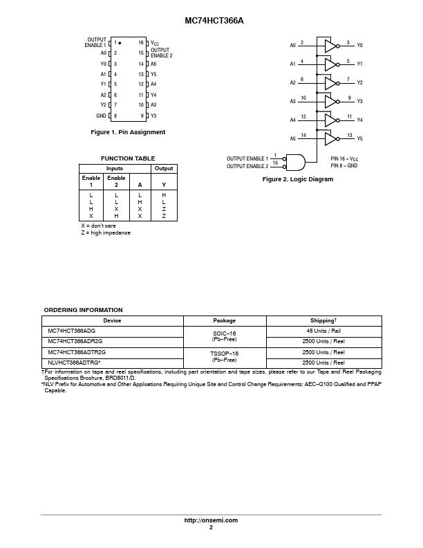
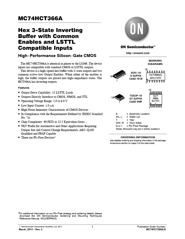
mance Silicon−Gate CMOS The MC74HCT366A is identical in pinout to the LS366. The device inputs are compatible with standard CMOS or LSTTL outputs. This device is a high−speed hex buffer with 3−state outputs and two common active−low Output Enables. When either of the enables is high, the buffer outputs are placed into high−impedance states. The HCT366A has inverting outputs. Features • Output Drive Capability: 15 LSTTL Loads • Outputs Directly Interface to CMOS, NMOS, and TTL • Operating Voltage Range: 2.0 to 6.0 V • Low Input Current: 1.0 mA • High Noise Immunity Characteristic of CMOS Devices • In Compliance with the Req
 MC74HCT366A Datasheet