Full PDF Text Transcription for MC74HCT365A (Reference)
Note: Below is a high-fidelity text extraction (approx. 800 characters) for
MC74HCT365A. For precise diagrams, and layout, please refer to the original PDF.
DATA SHEET www.onsemi.com Hex 3-State Noninverting Buffer with Common Enables High−Performance Silicon−Gate CMOS MC74HC365A, MC74HCT365A The MC74HC365A/MC74HCT365A is ide...
View more extracted text
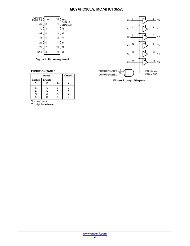
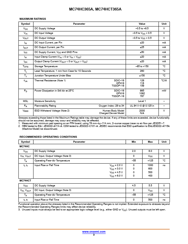
on−Gate CMOS MC74HC365A, MC74HCT365A The MC74HC365A/MC74HCT365A is identical in pinout to the LS365. The MC74HC365A inputs are compatible with standard CMOS outputs; with pullup resistors, they are compatible with LSTTL outputs. The MC74HCT365A inputs are compatible with LSTTL outputs. This device is a high−speed hex buffer with 3−state outputs and two common active−low Output Enables. When either of the enables is high, the buffer outputs are placed into high−impedance states. The HC365A, HCT365A has noninverting outputs. Features Output Drive Capability: 15 LSTTL Loads Outputs Directly Interface to CMOS, NMOS, and TT
 MC74HCT365A Datasheet