Datasheet Details
| Part number | FDMS1D2N03DSD |
|---|---|
| Manufacturer | onsemi |
| File Size | 505.46 KB |
| Description | Dual N-Channel MOSFETs |
| Datasheet |
 FDMS1D2N03DSD Datasheet FDMS1D2N03DSD Datasheet
|


|
|
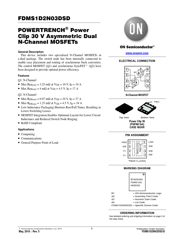
a dual package.
The switch node has been internally connected to enable easy placement and routing of synchronous buck converters.
The control MOSFET (Q1) and synchronous SyncFETt (Q2) have been designed to provide optimal power efficiency.
| Part number | FDMS1D2N03DSD |
|---|---|
| Manufacturer | onsemi |
| File Size | 505.46 KB |
| Description | Dual N-Channel MOSFETs |
| Datasheet |
FDMS1D2N03DSD Datasheet
|
|
|
|
| Part Number | Description |
|---|---|
| FDMS003N08C | N-Channel MOSFET |
| FDMS007N08LC | N-Channel MOSFET |
| FDMS030N06B | N-Channel MOSFET |
| FDMS0310AS | N-Channel MOSFET |
| FDMS0312AS | N-Channel MOSFET |
| FDMS0312S | N-Channel MOSFET |
| FDMS037N08B | N-Channel MOSFET |
| FDMS039N08B | N-Channel MOSFET |
| FDMS2572 | N-Channel MOSFET |
| FDMS2672 | N-Channel MOSFET |
The following content is an automatically extracted verbatim text from the original manufacturer datasheet and is provided for reference purposes only.