74HC595
Features
- Output Drive Capability: 15 LSTTL Loads
- Outputs Directly Interface to CMOS, NMOS, and TTL
- Operating Voltage Range: 2.0 to 6.0 V
- Low Input Current: 1.0 m A
- High Noise Immunity Characteristic of CMOS Devices
- In pliance with the Requirements Defined by JEDEC
Standard No. 7A
- ESD Performance: HBM > 2000 V; Machine Model > 200 V
- Chip plexity: 328 FETs or 82 Equivalent Gates
- Improvements over HC595
- Improved Propagation Delays
- 50% Lower Quiescent Power
- Improved Input Noise and Latchup Immunity
- These are Pb- Free Devices
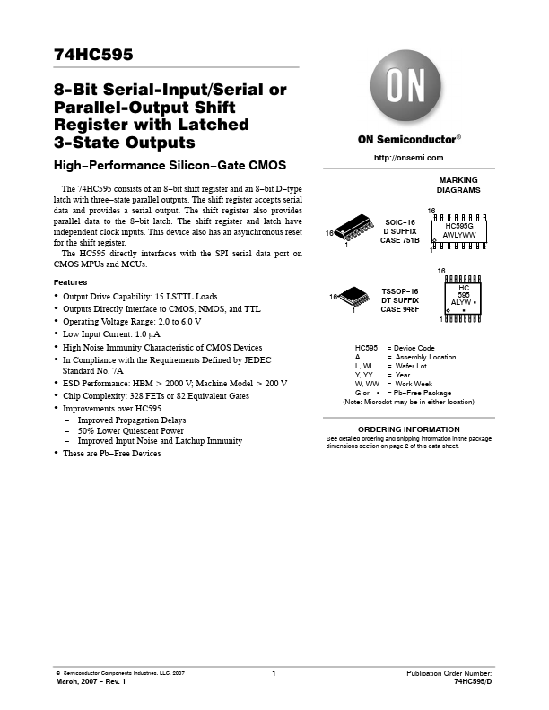
16 1
16 1 http://onsemi.
MARKING DIAGRAMS
SOIC- 16 D SUFFIX CASE 751B
HC595G AWLYWW
TSSOP- 16 DT SUFFIX CASE 948F
HC 595 ALYW G
G 1
HC595 = Device Code A = Assembly Location L, WL = Wafer Lot Y, YY = Year W, WW = Work Week G or G = Pb- Free Package (Note: Microdot may be in either location)
ORDERING INFORMATION
See detailed ordering and shipping information in the package dimensions section on page 2 of this data sheet.
©...

Representative 74HC595 image (package may vary by manufacturer)