74HC595
Description
This device each contains an 8-bit serial-in, parallel-out shift register that feeds an 8-bit D-type storage register. The storage register has parallel 3-state outputs. Separate clocks are provided for both the shift register and the storage register. The shift register has a direct-overriding clear, serial input, and serial output pins for cascading. Both the shift register and storage register clocks are positive-edge triggered. If the user wishes to connect both clocks together, the shift register state will always be one clock pulse ahead of the storage register.
Features
- -
- -
- High Speed Operation: tpd (RCK to Q) = 17 ns typ (C L = 50 p F) High Output Current: Fanout of 15 LSTTL Loads (QA to QH outputs) Wide Operating Voltage: VCC = 2 to 6 V Low Input Current: 1 µA max Low Quiescent Supply Current: ICC (static) = 4 µA max (Ta = 25°C)
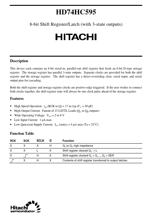
Function Table
RCK X X X X SCK X X SCLR X L H H G H X X X Function QA to QH high impedance Shift register cleared QH ’ = L Shift...

Representative 74HC595 image (package may vary by manufacturer)