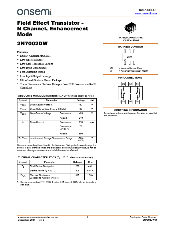
2N7002DW
Features
- Dual N-Channel MOSFET
- Low On-Resistance
- Low Gate Threshold Voltage
- Low Input Capacitance
- Fast Switching Speed
- Low Input/Output Leakage
- Ultra-Small Surface Mount Package
- These Devices are Pb-Free, Halogen Free/BFR Free and are Ro HS pliant
ABSOLUTE MAXIMUM RATINGS (TA = 25 C unless otherwise noted)
Symbol
Parameter
Ratings Unit
VDSS Drain-Source Voltage
VDGR Drain-Gate Voltage (RGS 1.0 MW)
VGSS Gate-Source Voltage
Continuous
20
Pulsed
40
Drain Current
Continuous
115 m A
Continuous
73 at 100 C
Pulsed
TJ, TSTG Junction and Storage Temperature Range
- 55 to
C
+150
Stresses exceeding those listed in the Maximum Ratings table may damage the device. If any of these limits are exceeded, device functionality should not be assumed, damage may occur and reliability may be affected.
THERMAL CHARACTERISTICS (TA = 25 C unless otherwise noted)
Symbol
Parameter
Ratings...