Datasheet Details
| Part number | DM74LS962 |
|---|---|
| Manufacturer | National |
| File Size | 157.99 KB |
| Description | Dual Rank 8-Bit TRI-STATE Shift Register |
| Datasheet |
 DM74LS962 Datasheet DM74LS962 Datasheet
|
|
|
| Part number | DM74LS962 |
|---|---|
| Manufacturer | National |
| File Size | 157.99 KB |
| Description | Dual Rank 8-Bit TRI-STATE Shift Register |
| Datasheet |
DM74LS962 Datasheet
|
|
|
|
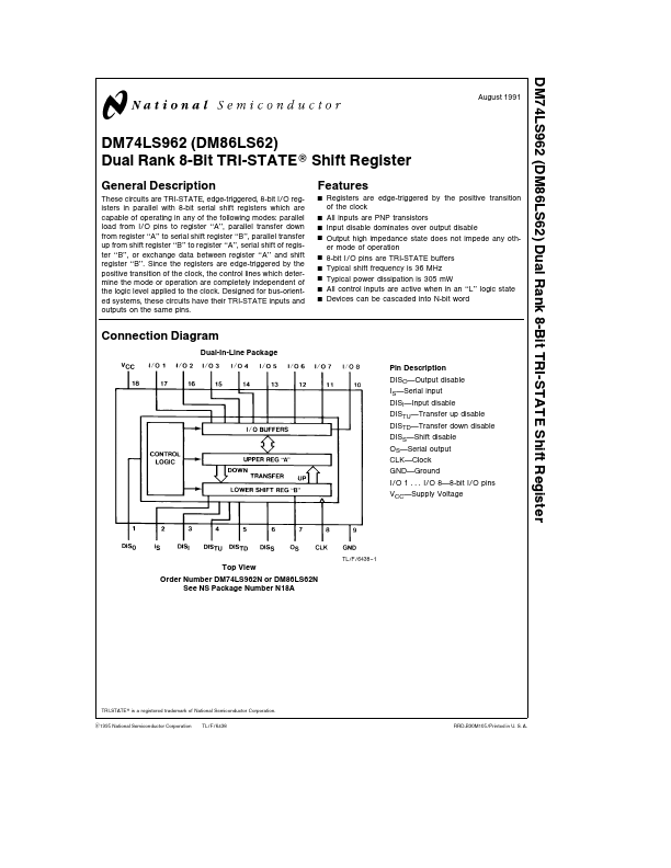
These circuits are TRI-STATE edge-triggered 8-bit I O registers in parallel with 8-bit serial shift registers which are capable of operating in any of the following modes parallel load from I O pins to register ‘‘A’’ parallel transfer down from register ‘‘A’’ to serial shift register ‘‘B’’ parallel transfer up from shift register ‘‘B’’ to register ‘‘A’’ serial shift of register ‘‘B’’ or exchange data between register ‘‘A’’ and shift register ‘‘B’’ Since the registers are edge-triggered by the positive transition of the clock the control lines which determine the mode or operation are completely independent of the logic level applied to the clock Designed for bus-oriented systems these circuits have their TRI-STATE inputs and outputs on the same pins
DM74LS962 (DM86LS62) Dual Rank 8-Bit TRI-STATE Shift Register August 1991 DM74LS962 (DM86LS62) Dual Rank 8-Bit TRI-STATE Shift.
| Part Number | Description |
|---|---|
| DM74LS96 | 5 Bit Shift Registers |
| DM74LS90 | Decade and Binary Counters |
| DM74LS93 | Decade and Binary Counters |
| DM74LS347 | BCD To 7 Segment Decoder / Driver |
| DM74ALS1011A | Triple 3 Input AND Buffer |
| DM74ALS1242A | Quad Bidirectional Bus Driver |
| DM74ALS1620 | Octal Tri-State Bus Transceivers |
| DM74ALS996 | D Type Edge Triggered Readback Latches |
| DM74AS1036A | Quad 2 Input NOR Driver |
| DM74AS282 | Look Ahead Carry Generator |