Datasheet Details
| Part number | DM74LS467 |
|---|---|
| Manufacturer | National Semiconductor (now Texas Instruments) |
| File Size | 118.10 KB |
| Description | (DM74LS465 - DM74LS468) TRI-STATE Octal Buffer |
| Datasheet |
 DM74LS467 Datasheet DM74LS467 Datasheet
|

|
|
Download the DM74LS467 datasheet PDF. This datasheet also covers the DM74LS466 variant, as both devices belong to the same (dm74ls465 - dm74ls468) tri-state octal buffer family and are provided as variant models within a single manufacturer datasheet.
| Part number | DM74LS467 |
|---|---|
| Manufacturer | National Semiconductor (now Texas Instruments) |
| File Size | 118.10 KB |
| Description | (DM74LS465 - DM74LS468) TRI-STATE Octal Buffer |
| Datasheet |
DM74LS467 Datasheet
|
|
|
|
Note: Below is a high-fidelity text extraction (approx. 800 characters) for DM74LS467. For precise diagrams, and layout, please refer to the original PDF.
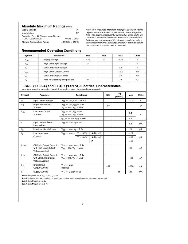
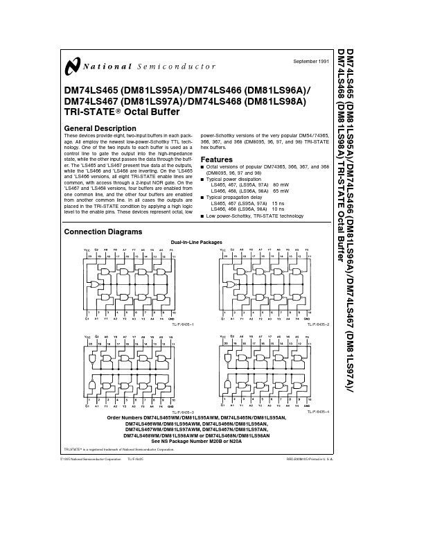
DM74LS465 (DM81LS95A) DM74LS466 (DM81LS96A) DM74LS467 (DM81LS97A) DM74LS468 (DM81LS98A) TRI-STATE Octal Buffer September 1991 DM74LS465 (DM81LS95A) DM74LS466 (DM81LS96A) ...
| Part Number | Description |
|---|---|
| DM74LS460 | 10-Bit Comparator |
| DM74LS461 | Octal Counter |
| DM74LS465 | (DM74LS465 - DM74LS468) TRI-STATE Octal Buffer |
| DM74LS466 | (DM74LS465 - DM74LS468) TRI-STATE Octal Buffer |
| DM74LS468 | (DM74LS465 - DM74LS468) TRI-STATE Octal Buffer |
| DM74LS40 | Dual 4-Input NAND Buffer |
| DM74LS42 | Decimal Decoders |
| DM74LS447 | BCD to 7-Segment Decoder/Driver |
| DM74LS450 | 16:1 Multiplexer |
| DM74LS451 | DM54LS451/DM74LS451 DUAL 8:1 Multiplexer |