Datasheet4U Logo Datasheet4U.com

NT5CC128M8DN - 1Gb DDR3 SDRAM

This page provides the datasheet information for the NT5CC128M8DN, a member of the NT5CB128M8DN 1Gb DDR3 SDRAM family.

Datasheet Summary

Description

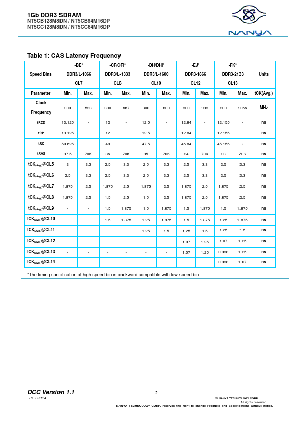
The 1Gb Double-Data-Rate-3 (DDR3/L) B-die DRAMs is double data rate architecture to achieve high-speed operation.

It is internally configured as an eight bank DRAM.

The 1Gb chip is organized as 16Mbit x 8 I/Os x 8 banks or 8Mbit x 16 I/Os x 8 bank devices.

Features

  • and all of the control and address inputs are synchronized with a pair of externally supplied differential clocks. Inputs are latched at the cross point of differential clocks (CK rising and falling). All I/Os are synchronized with a single ended DQS or differential DQS pair in a source synchronous fashion. These devices operate with a single 1.5V ± 0.075V or 1.35V -0.067/+0.1V power supply and are available in BGA packages. DCC Version 1.1 01 / 2014 3 © NANYA.

📥 Download Datasheet

Datasheet preview – NT5CC128M8DN

Datasheet Details

Part number NT5CC128M8DN
Manufacturer Nanya
File Size 2.62 MB
Description 1Gb DDR3 SDRAM
Datasheet download datasheet NT5CC128M8DN Datasheet
Additional preview pages of the NT5CC128M8DN datasheet.
Other Datasheets by Nanya

Full PDF Text Transcription

Click to expand full text
1Gb DDR3 SDRAM NT5CB128M8DN / NT5CB64M16DP NT5CC128M8DN / NT5CC64M16DP Feature  1.5V ± 0.075V & 1.35V -0.067/+0.1V (JEDEC Standard Power Supply)  VDD= VDDQ= 1.35V (1.283~1.45V ) Backward compatible to VDD= VDDQ= 1.5V ±0.075V Supports DDR3L devices to be backward compatible in 1.
Published: |