BUK98150-55
DESCRIPTION
N-channel enhancement mode logic level field-effect power transistor in a plastic envelope suitable for surface mounting. The device features very low on-state resistance and has integral zener diodes giving ESD protection. It is intended for use in automotive and general purpose switching applications.
QUICK REFERENCE DATA
SYMBOL VDS ID Ptot Tj RDS(ON) PARAMETER Drain-source voltage Drain current Total power dissipation Junction temperature Drain-source on-state resistance VGS = 5 V MAX. 55 5.5 1.8 150 150 UNIT V A W ˚C mΩ
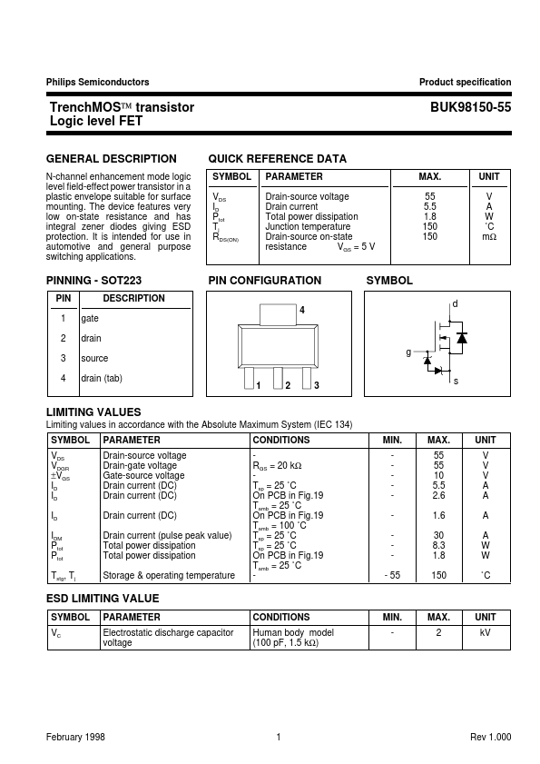
PINNING
- SOT223
PIN 1 2 3 4 gate drain source drain (tab) DESCRIPTION
PIN CONFIGURATION
SYMBOL d g s
LIMITING VALUES
Limiting values in accordance with the Absolute Maximum System (IEC 134) SYMBOL VDS VDGR ±VGS ID ID ID IDM Ptot Ptot Tstg, Tj PARAMETER Drain-source voltage Drain-gate voltage Gate-source voltage Drain current (DC) Drain current (DC) Drain current (DC) Drain current (pulse peak value) Total power dissipation...