Datasheet Details
| Part number | 74AUP1T58 |
|---|---|
| Manufacturer | NXP Semiconductors |
| File Size | 136.23 KB |
| Description | Low-power Configurable Gate |
| Datasheet |
 74AUP1T58 Datasheet 74AUP1T58 Datasheet
|
|
|
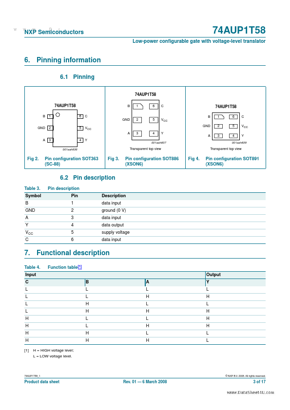
The 74AUP1T58 provides low-power, low-voltage configurable logic gate functions.
The output state is determined by eight patterns of 3-bit input.
The user can choose the logic functions AND, OR, NAND, NOR, XOR, inverter and buffer.
| Part number | 74AUP1T58 |
|---|---|
| Manufacturer | NXP Semiconductors |
| File Size | 136.23 KB |
| Description | Low-power Configurable Gate |
| Datasheet |
74AUP1T58 Datasheet
|
|
|
|
| Part Number | Description | Manufacturer |
|---|---|---|
| 74AUP1T58 | Low-power configurable gate | nexperia |
| 74AUP1T50 | Low-power buffer | nexperia |
| 74AUP1T57 | Low-power configurable gate | nexperia |
| 74AUP1T00 | Low-power 2-input NAND gate | nexperia |
| 74AUP1T02 | Low-power 2-input NOR gate | nexperia |
| Part Number | Description |
|---|---|
| 74AUP1T57 | Low-power Configurable Gate |
| 74AUP1G02 | Low-power 2-input NOR gate |
| 74AUP1G0832 | Low Power 3-Input AND-OR Gate |
| 74AUP1G09 | Low-power 2-input AND Gate |
| 74AUP1G11 | Low-power 3-input AND gate |
The following content is an automatically extracted verbatim text from the original manufacturer datasheet and is provided for reference purposes only.