Click to expand full text
www.DataSheet4U.com
74AUP1T57
Low-power configurable gate with voltage-level translator
Rev. 01 — 3 January 2008 Product data sheet
1. General description
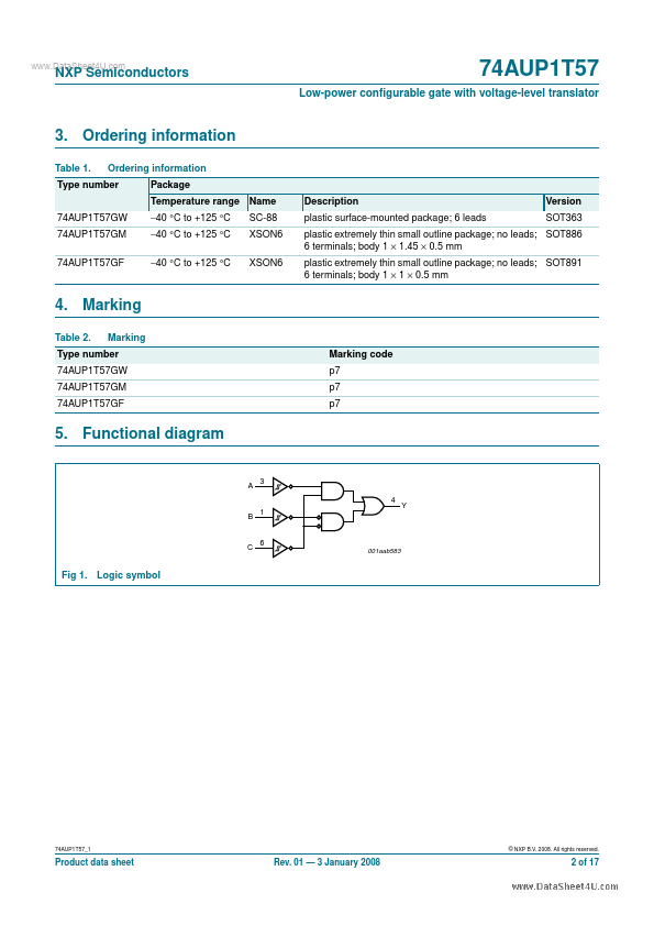
The 74AUP1T57 provides low-power, low-voltage configurable logic gate functions. The output state is determined by eight patterns of 3-bit input. The user can choose the logic functions AND, OR, NAND, NOR, XNOR, inverter and buffer. All inputs can be connected to VCC or GND. This device ensures a very low static and dynamic power consumption across the entire VCC range from 2.3 V to 3.6 V. The 74AUP1T57 is designed for logic-level translation applications with input switching levels that accept 1.8 V low-voltage CMOS signals, while operating from either a single 2.5 V or 3.3 V supply voltage.
 74AUP1T57 Datasheet