Click to expand full text
74LVC2G240
Dual inverting buffer/line driver; 3-state
Rev. 04 — 29 February 2008
www.DataSheet4U.com
Product data sheet
1. General description
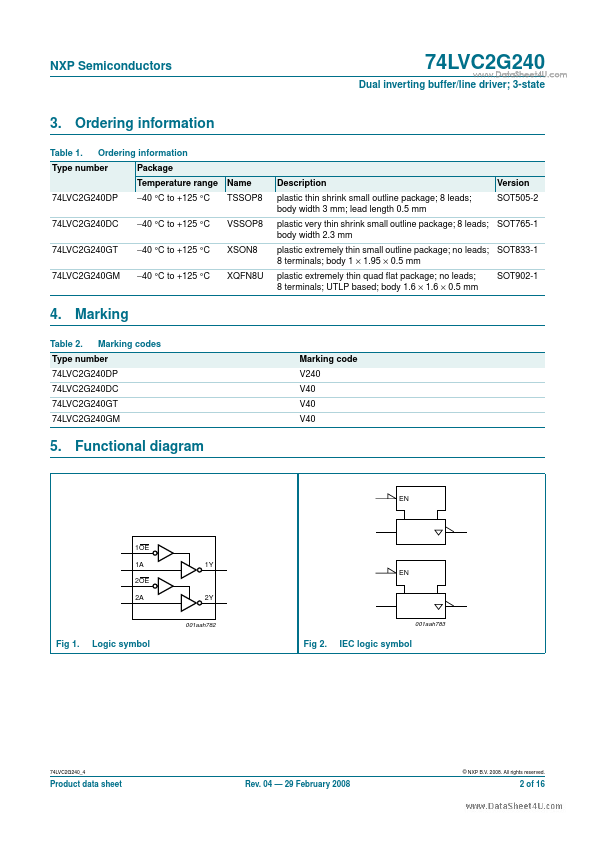
The 74LVC2G240 is a dual inverting buffer/line driver with 3-state outputs. The 3-state outputs are controlled by the output enable inputs 1OE and 2OE. A HIGH level at pins nOE causes the outputs to assume a high-impedance OFF-state. Schmitt trigger action at all inputs makes the circuit highly tolerant of slower input rise and fall times. Inputs can be driven from either 3.3 V or 5 V devices. This feature allows the use of the 74LVC2G240 as a translator in a mixed 3.3 V and 5 V environment. It is fully specified for partial power-down applications using IOFF.
 74LVC2G240 Datasheet