Click to expand full text
NIKO-SEM
N-Channel Enhancement Mode
PK6A8BA
Field Effect Transistor
PDFN 5x6P
Halogen-Free & Lead-Free
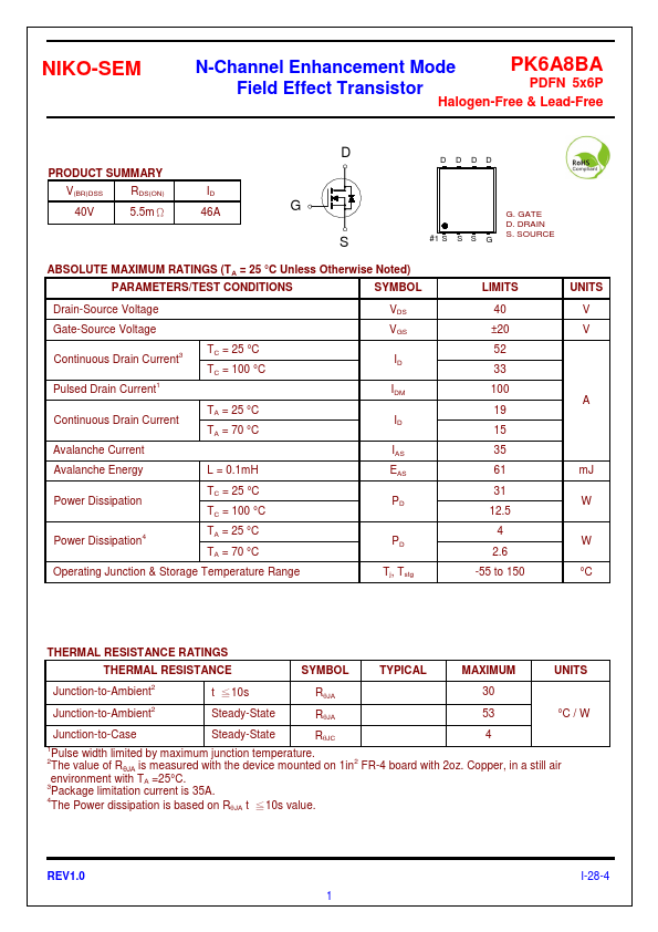
PRODUCT SUMMARY
V(BR)DSS
RDS(ON)
40V
5.5mΩ
ID 46A
D
G S
D D DD
#1 S S S G
G. GATE D. DRAIN S. SOURCE
ABSOLUTE MAXIMUM RATINGS (TA = 25 °C Unless Otherwise Noted)
PARAMETERS/TEST CONDITIONS
SYMBOL
Drain-Source Voltage
Gate-Source Voltage
Continuous Drain Current3 Pulsed Drain Current1
TC = 25 °C TC = 100 °C
Continuous Drain Current
TA = 25 °C TA = 70 °C
Avalanche Current
Avalanche Energy
L = 0.1mH
Power Dissipation
TC = 25 °C TC = 100 °C
Power Dissipation4
TA = 25 °C TA = 70 °C
Operating Junction & Storage Temperature Range
VDS VGS ID IDM ID IAS EAS PD
PD Tj, Tstg
LIMITS 40 ±20 52 33 100 19 15 35 61 31 12.5 4 2.
 PK6A8BA Datasheet