Datasheet Details
| Part number | PD5C1BA |
|---|---|
| Manufacturer | NIKO-SEM |
| File Size | 341.71 KB |
| Description | P-Channel Enhancement Mode Field Effect Transistor |
| Datasheet |
 PD5C1BA Datasheet PD5C1BA Datasheet
|
|
|
Download the PD5C1BA datasheet PDF. This datasheet also covers the PD5C1BA-NIKO variant, as both devices belong to the same p-channel enhancement mode field effect transistor family and are provided as variant models within a single manufacturer datasheet.

| Part number | PD5C1BA |
|---|---|
| Manufacturer | NIKO-SEM |
| File Size | 341.71 KB |
| Description | P-Channel Enhancement Mode Field Effect Transistor |
| Datasheet |
PD5C1BA Datasheet
|
|
|
|
Note: Below is a high-fidelity text extraction (approx. 800 characters) for PD5C1BA. For precise diagrams, and layout, please refer to the original PDF.
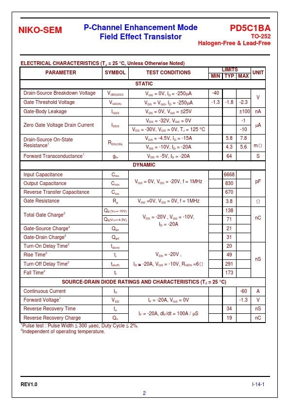
NIKO-SEM P-Channel Enhancement Mode PD5C1BA Field Effect Transistor TO-252 Halogen-Free & Lead-Free PRODUCT SUMMARY V(BR)DSS RDS(ON) -40V 5.6mΩ ID -88A Features • Pb−Free...
| Part Number | Description |
|---|---|
| PD5G3EA | P-Channel Enhancement Mode Field Effect Transistor |