2SK2157
FEATURES
- New package intermediate between small-signal and power models
- Can be directly driven by output of 5-V IC
- Low ON resistance RDS(on) ≤ 0.15 Ω @VGS = 4 V, ID = 2.5 A RDS(on) ≤ 0.10 Ω @VGS = 10 V, ID = 2.5 A
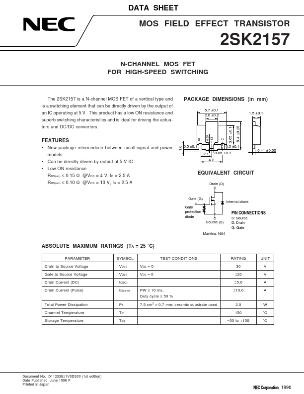
S 0.5 ±0.1
0.5 ±0.1 2.1 4.2 0.85 ±0.1
0.41 ±0.05
EQUIVALENT CIRCUIT
Drain (D)
Gate (G) Gate protection diode Source (S) Marking: NA4
Internal diode PIN CONNECTIONS S: Source D: Drain G: Gate
ABSOLUTE MAXIMUM RATINGS (TA = 25 ˚C)
PARAMETER Drain to Source Voltage Gate to Source Voltage Drain Current (DC) Drain Current (Pulse) SYMBOL VDSS VGSS ID(DC) ID(pulse) PW ≤ 10 ms, Duty cycle ≤ 50 % 7.5 cm2 × 0.7 mm, ceramic substrate used VGS = 0 VDS = 0 TEST CONDITIONS RATING 30 ± 20 ± 5.0 ± 10.0 UNIT V V A A
Total Power Dissipation Channel Temperature Storage Temperature
PT Tch Tstg
2.0 150
- 55 to +150
W ˚C ˚C
Document No. D11233EJ1V0DS00 (1st edition) Date Published June 1996 P Printed in Japan
ELECTRICAL CHARACTERISTICS (TA = 25...