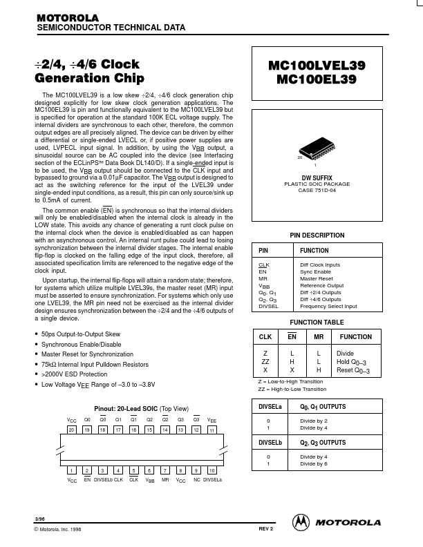
PIN CLK EN MR VBB Q0, Q1 Q2, Q3 DIVSEL FUNCTION Diff Clock Inputs Sync Enable Master Reset Reference Output Diff ÷2/4 Outputs Diff ÷4/6 Outputs Frequency Select Input
FUNCTION TABLE CLK Z ZZ X EN L H X MR L L H FUNCTION Divide Hold Q0
3 Reset Q0
3
Full PDF Text Transcription for MC100LVEL39 (Reference)
Note: Below is a high-fidelity text extraction (approx. 800 characters) for
MC100LVEL39. For precise diagrams, and layout, please refer to the original PDF.
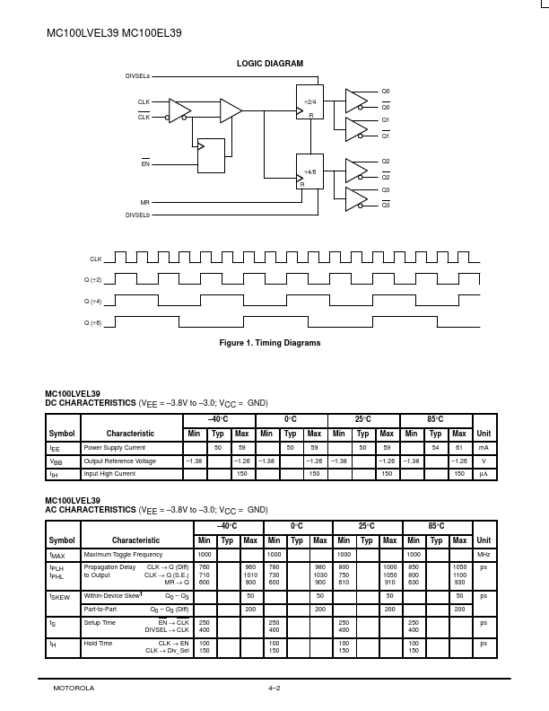
MOTOROLA SEMICONDUCTOR TECHNICAL DATA ÷2/4, ÷4/6 Clock MC100LVEL39 MC100EL39 Generation Chip The MC100LVEL39 is a low skew ÷2/4, ÷4/6 clock generation chip designed expli...
View more extracted text
00LVEL39 is a low skew ÷2/4, ÷4/6 clock generation chip designed explicitly for low skew clock generation applications. The MC100EL39 is pin and functionally equivalent to the MC100LVEL39 but is specified for operation at the standard 100K ECL voltage supply. The internal dividers are synchronous to each other, therefore, the common output edges are all precisely aligned. The device can be driven by either a differential or single-ended LVECL or, if positive power supplies are used, LVPECL input signal. In addition, by using the VBB output, a sinusoidal source can be AC coupled into the device (see Interfacing section of t
 MC100LVEL39 Datasheet