XP1003
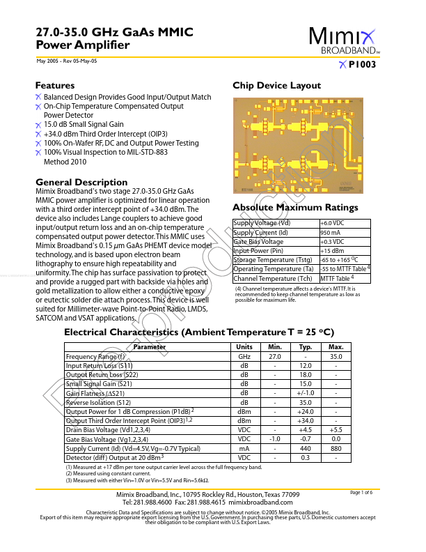
Features
Balanced Design Provides Good Input/Output Match On-Chip Temperature pensated Output Power Detector 15.0 d B Small Signal Gain +34.0 d Bm Third Order Intercept (OIP3) 100% On-Wafer RF, DC and Output Power Testing 100% Visual Inspection to MIL-STD-883 Method 2010
Electrical Characteristics (Ambient Temperature T = 25 o C)
Parameter Frequency Range (f ) Input Return Loss (S11) Output Return Loss (S22) Small Signal Gain (S21) Gain Flatness (∆S21) Reverse Isolation (S12) Output Power for 1 d B pression (P1d B) 2 Output Third Order Intercept Point (OIP3) 1,2 Drain Bias Voltage (Vd1,2,3,4) Gate Bias Voltage (Vg1,2,3,4) Supply Current (Id) (Vd=4.5V, Vg=-0.7V Typical) Detector (diff ) Output at 20 d Bm 3
Units GHz d B d B d B d B d B d Bm d Bm VDC VDC m A VDC Min. 27.0 -1.0 Typ. 12.0 18.0 15.0 +/-1.0 35.0 +24.0 +34.0 +4.5 -0.7 440 0.3 Max. 35.0 +5.5 0.0 880
- Pr
(1) Measured at +17 d Bm per tone output carrier level across the full frequency band. (2) Measured using constant current. (3)...