Click to expand full text
ZL30281
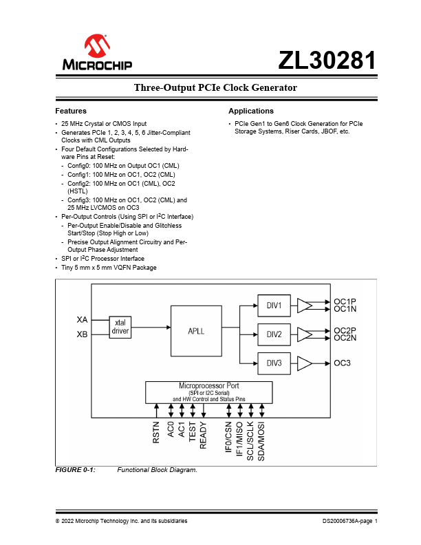
Three-Output PCIe Clock Generator
Features
• 25 MHz Crystal or CMOS Input
• Generates PCIe 1, 2, 3, 4, 5, 6 Jitter-Compliant Clocks with CML Outputs
• Four Default Configurations Selected by Hardware Pins at Reset:
- Config0: 100 MHz on Output OC1 (CML)
- Config1: 100 MHz on OC1, OC2 (CML)
- Config2: 100 MHz on OC1 (CML), OC2 (HSTL)
- Config3: 100 MHz on OC1, OC2 (CML) and 25 MHz LVCMOS on OC3
• Per-Output Controls (Using SPI or I2C Interface)
- Per-Output Enable/Disable and Glitchless Start/Stop (Stop High or Low)
- Precise Output Alignment Circuitry and PerOutput Phase Adjustment
• SPI or I2C Processor Interface
• Tiny 5 mm x 5 mm VQFN Package
Applications
• PCIe Gen1 to Gen6 Clock Generation for PCIe Storage Systems, Riser Cards, JBOF, etc.
 ZL30281 Datasheet