Click to expand full text
Register Map: Section 6.2
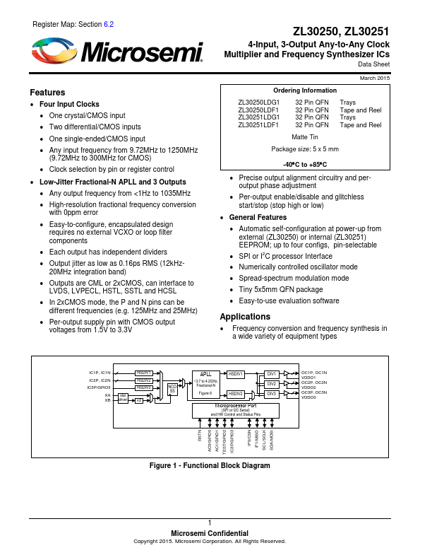
Features
Four Input Clocks One crystal/CMOS input Two differential/CMOS inputs One single-ended/CMOS input Any input frequency from 9.72MHz to 1250MHz (9.72MHz to 300MHz for CMOS) Clock selection by pin or register control
Low-Jitter Fractional-N APLL and 3 Outputs Any output frequency from <1Hz to 1035MHz High-resolution fractional frequency conversion with 0ppm error Easy-to-configure, encapsulated design requires no external VCXO or loop filter components Each output has independent dividers Output jitter as low as 0.16ps RMS (12kHz20MHz integration band) Outputs are CML or 2xCMOS, can interface to LVDS, LVPECL, HSTL, SSTL and HCSL In 2xCMOS mode, the P and N pins can be different frequencies (e.g.
 ZL30250 Datasheet