Absolute Maximum Ratings Ta = 25℃
Drain-Source Voltage Gate-Source Voltage
Parameter
Continuous Drain Current
Pulsed Drain Current
Power Dissipation
Thermal Resistance. Junction- to-Ambient Junction Temperature Junction St.
The following content is an automatically extracted verbatim text
from the original manufacturer datasheet and is provided for reference purposes only.
View original datasheet text
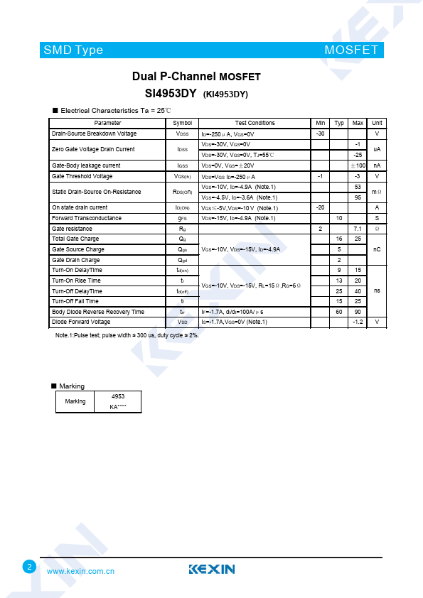
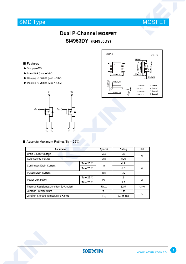
SMD Type
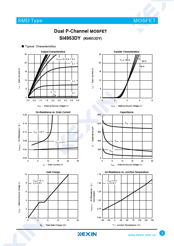
Dual P-Channel MOSFET SI4953DY (KI4953DY)
■ Features
● VDS (V) =-30V ● ID =-4.9 A (VGS =-10V) ● RDS(ON) < 53mΩ (VGS =-10V) ● RDS(ON) < 95mΩ (VGS =-4.5V)
S1
S2
+0.04 0.21 -0.02
SOP-8
G1
G2
MOSFET
1.50 0.15
1 Source1 2 Gate1 3 Source2 4 Gate2
5 Drain2 6 Drain2 7 Drain1 8 Drain1
D1 D1
D2 D2
■ Absolute Maximum Ratings Ta = 25℃
Drain-Source Voltage Gate-Source Voltage
Parameter
Continuous Drain Current
Pulsed Drain Current
Power Dissipation
Thermal Resistance.Junction- to-Ambient Junction Temperature Junction Storage Temperature Range
Ta = 25 ℃ Ta = 70 ℃
Ta = 25 ℃ Ta = 70 ℃
Symbol VDS VGS
ID
IDM
PD
RthJA TJ Tstg
Rating -30 ±20 -4.9 -3.9 -30 2 1.3 62.5 150
-55 to 150
Unit V
A
W ℃/W
℃
www.kexin.com.
 SI4953DY Datasheet