Datasheet4U Logo Datasheet4U.com

K2111 - MOS Field Effect Transistor

Key Features

  • Low on-resistance RDS(on)=0.6 MAX. @VGS=4.0V,ID=0.5A High switching speed SOT-89 4.50+0.1 -0.1 1.80+0.1 -0.1 12 3 0.48+0.1 -0.1 0.53+0.1 -0.1 +0.12.50 -0.1 +0.14.00 -0.1 Unit: mm 1.50+0.1 -0.1 0.44+0.1 -0.1 +0.10.80 -0.1 +0.12.60 -0.1 3.00+0.1 -0.1 Absolute Maximum Ratings Ta = 25 Parameter Drain to source voltage Gate to source voltage Drain current Power dissipation.
  • Channel temperature Storage temperature.
  • 16 cm2X0.7mm,ceramic substrate used Symbol VDSS VGSS ID Idp PD Tch T.

📥 Download Datasheet

Full PDF Text Transcription for K2111 (Reference)

Note: Below is a high-fidelity text extraction (approx. 800 characters) for K2111. For precise diagrams, and layout, please refer to the original PDF.

SMD Type MOS Field Effect Transistor 2SK2111 MOSFICET Features 
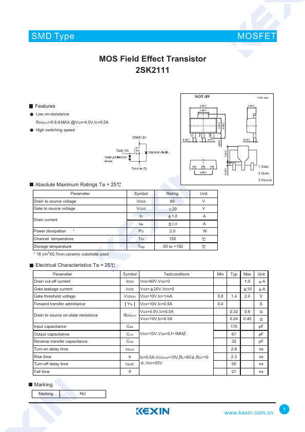
Low on-resistance RDS(on)=0.6 MAX.@VGS=4.0V,ID=0.5A High switching speed SOT-89 4.50+0.1 -0.1 1.80+0.1 -0.1...

View more extracted text
S=4.0V,ID=0.5A High switching speed SOT-89 4.50+0.1 -0.1 1.80+0.1 -0.1 12 3 0.48+0.1 -0.1 0.53+0.1 -0.1 +0.12.50 -0.1 +0.14.00 -0.1 Unit: mm 1.50+0.1 -0.1 0.44+0.1 -0.1 +0.10.80 -0.1 +0.12.60 -0.1 3.00+0.1 -0.1 Absolute Maximum Ratings Ta = 25 Parameter Drain to source voltage Gate to source voltage Drain current Power dissipation * Channel temperature Storage temperature * 16 cm2X0.7mm,ceramic substrate used Symbol VDSS VGSS ID Idp PD Tch Tstg Rating 60 20 1.0 2.0 2.