The following content is an automatically extracted verbatim text
from the original manufacturer datasheet and is provided for reference purposes only.
View original datasheet text
SMD Type
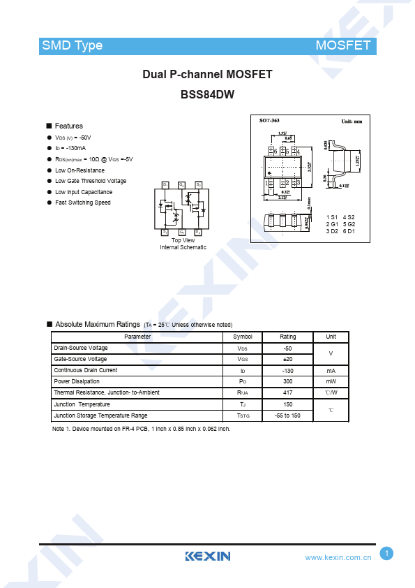
Dual P-channel MOSFET BSS84DW
■ Features
● VDS (V) = -50V ● ID = -130mA ● RDS(on)max = 10Ω @ VGS =-5V ● Low On-Resistance ● Low Gate Threshold Voltage ● Low Input Capacitance ● Fast Switching Speed
D1
G2
S2
S1
G1
D2
Top View Internal Schematic
MOSFET
1 S1 4 S2 2 G1 5 G2 3 D2 6 D1
■ Absolute Maximum Ratings (TA = 25℃ Unless otherwise noted)
Parameter Drain-Source Voltage Gate-Source Voltage Continuous Drain Current Power Dissipation Thermal Resistance, Junction- to-Ambient Junction Temperature Junction Storage Temperature Range
Symbol VDS VGS ID PD RᶿJA TJ TST G
Note 1. Device mounted on FR-4 PCB, 1 inch x 0.85 inch x 0.062 inch.
Rating -50 ±20 -130 300 417 150
-55 to 150
Unit V
mA mW ℃/W
℃
www.kexin.com.
 BSS84DW Datasheet