The following content is an automatically extracted verbatim text
from the original manufacturer datasheet and is provided for reference purposes only.
View original datasheet text
SMD Type
MOSFICET
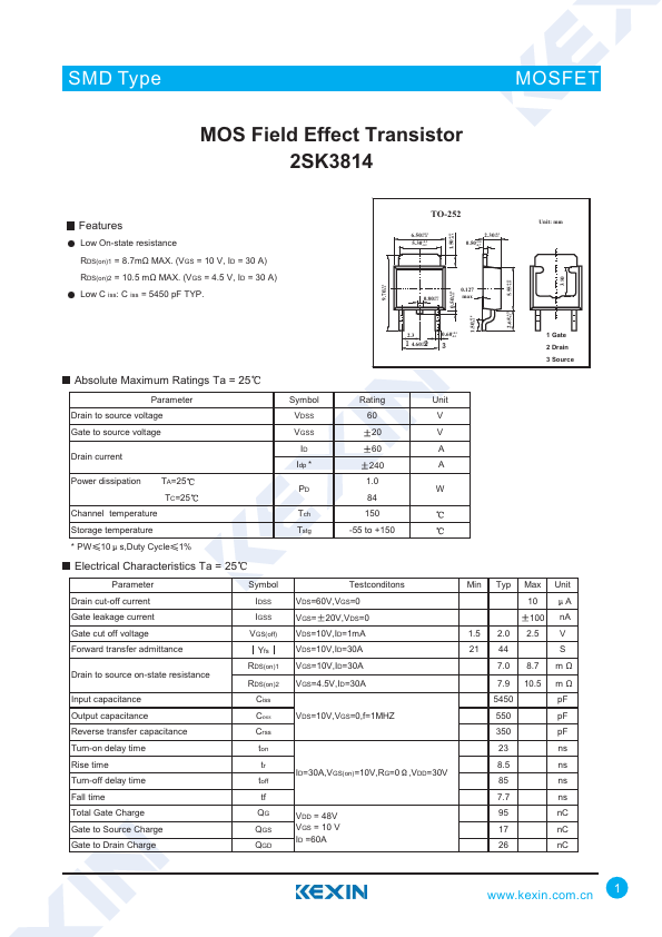
MOS Field Effect Transistor 2SK3814
Features
Low On-state resistance RDS(on)1 = 8.7mÙ MAX. (VGS = 10 V, ID = 30 A) RDS(on)2 = 10.5 mÙ MAX. (VGS = 4.5 V, ID = 30 A) Low C iss: C iss = 5450 pF TYP.
+0.2 9.70 -0.2
TO-252
6.50+0.15 -0.15
5.30+0.2 -0.2
2.30+0.1 -0.1
0.50+0.8 -0.7
Unit: mm
+0.15 1.50 -0.15
+0.15 5.55 -0.15
0.80+0.1 -0.1
0.127 max
3.80
+0.25 2.65 -0.1
+0.15 0.50 -0.15
+0.28 1.50 -0.1
2.3 4.60+0.15
-0.15
0.60+0.1 -0.1
1 Gate 2 Drain 3 Source
Absolute Maximum Ratings Ta = 25
Parameter Drain to source voltage Gate to source voltage
Drain current
Power dissipation TA=25 TC=25
Channel temperature Storage temperature * PW 10 s,Duty Cycle 1%
Symbol
Rating
Unit
VDSS
60
V
VGSS
20
V
ID
60
A
Idp *
240
A
1.
 2SK3814 Datasheet