Absolute Maximum Ratings Ta = 25℃
Parameter
Drain-Source Voltage
Drain-Gate Voltage @ RGS ≤ 1MΩ
Gate-Source Voltage
Continuous Pulsed
Continuous
Continuous Drain Current
Continuous @ 100°C
Pulsed
Power Dissipation
Derating above Ta = 25°C
Thermal Resistance. Junction- to-Ambient.
The following content is an automatically extracted verbatim text
from the original manufacturer datasheet and is provided for reference purposes only.
View original datasheet text
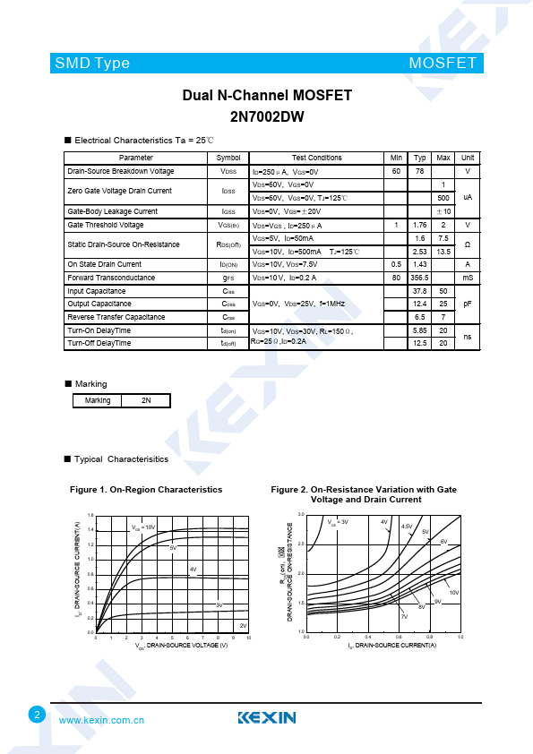
SMD Type
Dual N-Channel MOSFET 2N7002DW
■ Features
● VDS (V) = 60V ● ID = 115 mA (VGS = 10V) ● RDS(ON) < 7.5 Ω (VGS = 5V) ● Low Input Capacitance ● Fast Switching Speed ● Low On-Resistance
MOSFET
1.S2 4.S1 2.G2 5.G1 3.D1 6.D2
■ Absolute Maximum Ratings Ta = 25℃
Parameter
Drain-Source Voltage
Drain-Gate Voltage @ RGS ≤ 1MΩ
Gate-Source Voltage
Continuous Pulsed
Continuous
Continuous Drain Current
Continuous @ 100°C
Pulsed
Power Dissipation
Derating above Ta = 25°C
Thermal Resistance.Junction- to-Ambient
Junction Temperature
Storage Temperature Range
Symbol VDS VDG VGS
ID
PD RthJA
TJ Tstg
Rating 60 60 ±20 ±40 115 73 800 200 1.6 625 150
-55 to 150
Unit
V
mA mW mW/℃ ℃/W ℃
www.kexin.com.
 2N7002DW Datasheet