Absolute Maximum Ratings (Ta = 25°C unless otherwise noted)
Parameter Drain-Source Voltage Gate-Source Voltage Continuous Drain Current Pulsed Drain Current (tp=10μs) Power Dissipation (Note 1) Thermal Resistance. Junction- to-Ambient (Note 1) Junction Temperature Storage Temperature Range
Symbol VDS VGS ID.
The following content is an automatically extracted verbatim text
from the original manufacturer datasheet and is provided for reference purposes only.
View original datasheet text
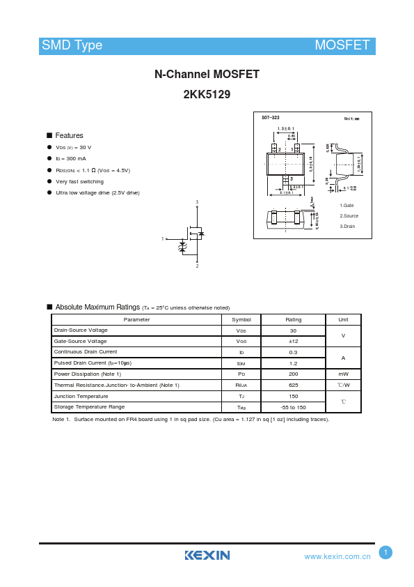
SMD Type
N-Channel MOSFET 2KK5129
■ Features
● VDS (V) = 30 V ● ID = 300 mA ● RDS(ON) < 1.1 Ω (VGS = 4.5V) ● Very fast switching ● Ultra low voltage drive (2.5V drive)
3
1 2
MOSFET
1.Gate 2.Source 3.Drain
■ Absolute Maximum Ratings (Ta = 25°C unless otherwise noted)
Parameter Drain-Source Voltage Gate-Source Voltage Continuous Drain Current Pulsed Drain Current (tp=10μs) Power Dissipation (Note 1) Thermal Resistance.Junction- to-Ambient (Note 1) Junction Temperature Storage Temperature Range
Symbol VDS VGS ID IDM PD RθJA TJ Tstg
Rating 30 ±12 0.3 1.2 200 625 150
-55 to 150
Unit V
A mW ℃/W ℃
Note 1. Surface mounted on FR4 board using 1 in sq pad size. (Cu area = 1.127 in sq [1 oz] including traces).
www.kexin.com.
 2KK5129 Datasheet