Click to expand full text
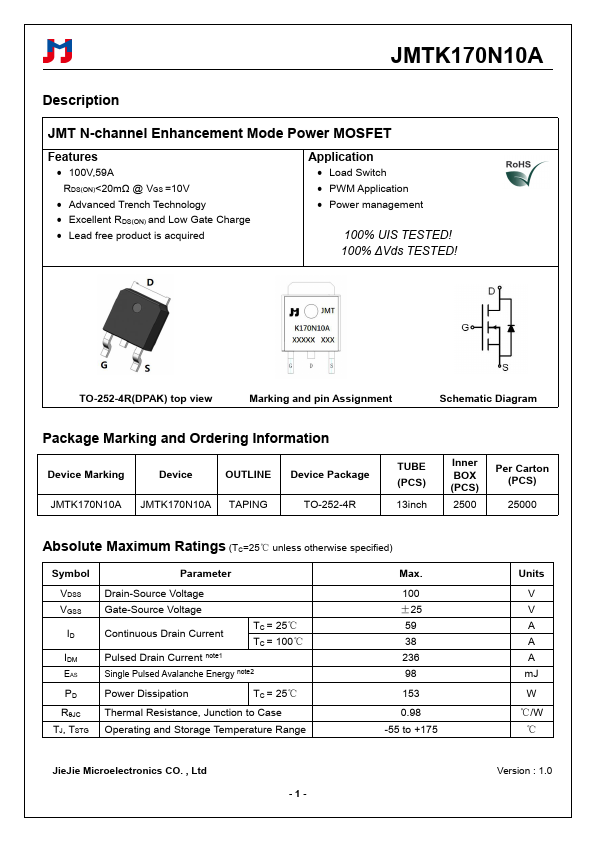
JMTK170N10A
Description
JMT N-channel Enhancement Mode Power MOSFET
Features
100V,59A RDS(ON)<20mΩ @ VGS =10V
Advanced Trench Technology Excellent RDS(ON) and Low Gate Charge Lead free product is acquired
Application
Load Switch PWM Application Power management
100% UIS TESTED! 100% ΔVds TESTED!
TO-252-4R(DPAK) top view
Marking and pin Assignment
Schematic Diagram
Package Marking and Ordering Information
Device Marking
Device
OUTLINE Device Package
JMTK170N10A JMTK170N10A TAPING
TO-252-4R
TUBE (PCS)
13inch
Inner BOX (PCS)
2500
Per Carton (PCS)
25000
Absolute Maximum Ratings (TC=25℃ unless otherwise specified)
Symbol VDSS VGSS
ID
IDM
EAS
PD RθJC TJ, TSTG
Parameter
Drain-Source Voltage
Gate-Source Voltage
Continuous Drain Current
TC = 25℃ TC = 100℃
Pulse
 JMTK170N10A Datasheet