2N7002W
FEATURE z High density cell design for low RDS(ON) z Voltage controlled small signal switch z Rugged and reliable z High saturation current capability
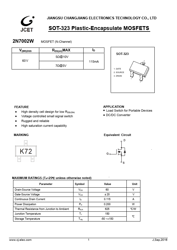
MARKING
APPLICATION z Load Switch for Portable Devices z DC/DC Converter
Equivalent Circuit
MAXIMUM RATINGS (Ta=25℃ unless otherwise noted)
Parameter
Symbol
Drain-Source Voltage
Gate-Source Voltage
Continuous Drain Current
Power Dissipation
Thermal Resistance from Junction to Ambient
RθJA
Junction Temperature
Storage Temperature
Tstg
Value 60 ± 20
0.115 0.200 625 150 -50 ~+150
Unit V V A W ℃/W
℃
.cj-elec.
J,Sep,2016
MOSFET ELECTRICAL CHARACTERISTICS
Ta=25 ℃ unless otherwise specified
Parameter
Symbol
Test conditions
Drain-Source Breakdown Voltage Gate-Threshold Voltage Gate-body Leakage Zero Gate Voltage Drain Current On-state Drain Current
Drain-Source On-Resistance
Forward Trans conductance
Drain-source on-voltage
Diode Forward Voltage Input Capacitance
- Output Capacitance
- Reverse...