Click to expand full text
www.DataSheet4U.com
2.5V LVDS, 1:4 GLITCHLESS CLOCK BUFFER TERABUFFER™ II General Description
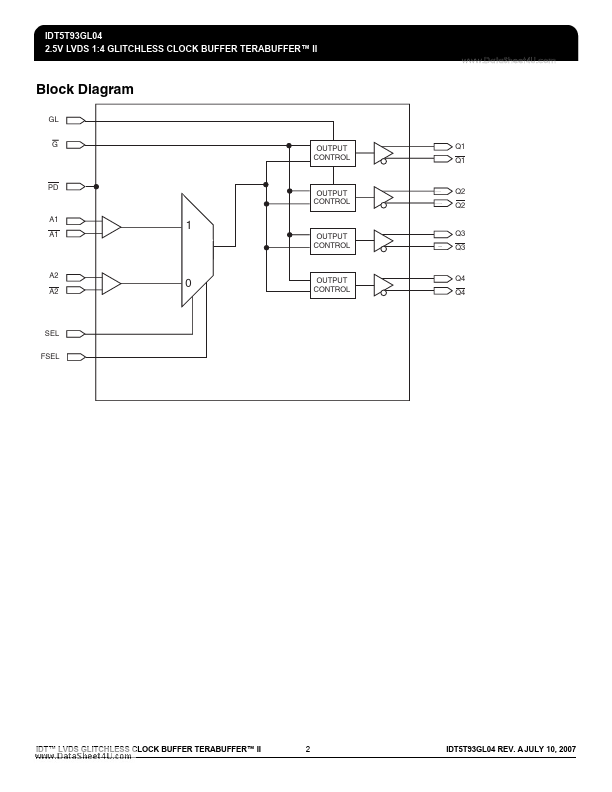
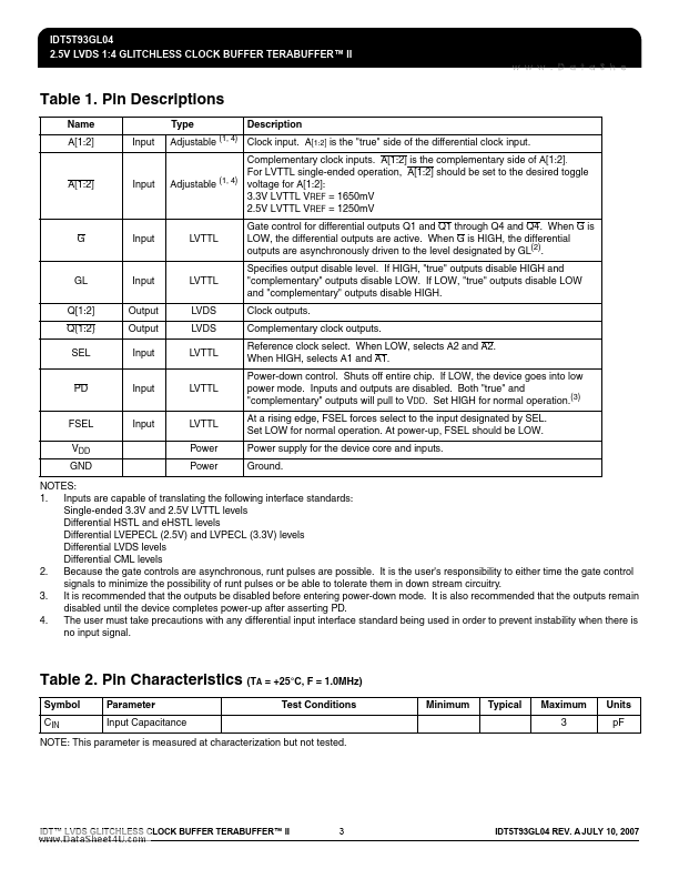
The IDT5T93GL04 2.5V differential clock buffer is a user-selectable differential input to four LVDS outputs. The fanout from a differential input to four LVDS outputs reduces loading on the preceding driver and provides an efficient clock distribution network. The IDT5T93GL04 can act as a translator from a differential HSTL, eHSTL, LVEPECL (2.5V), LVPECL (3.3V), CML, or LVDS input to LVDS outputs. A single-ended 3.3V / 2.5V LVTTL input can also be used to translate to LVDS outputs. The redundant input capability allows for a glitchless change-over from a primary clock source to a secondary clock source up to 450MHz. Selectable inputs are controlled by SEL.
 IDT5T93GL04 Datasheet