Click to expand full text
PRELIMINARY INFORMATION
ICSLV218
www.DataSheet4U.com
Dual 1-to-8 Low Voltage Clock Buffer/Translator
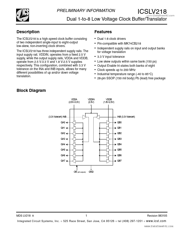
Description
The ICSLV218 is a high-speed clock buffer consisting of two independent single-input to eight-output low-skew, non-inverting clock drivers. The ICSLV218 has three independent supply rails: The input supply rail, VDDIN, operates from a fixed 2.5 V supply, while the output supply rails, VDDA and VDDB, operate from 2.5 V-3.3 V and 1.8 V-2.5 V supplies respectively. This configuration, combined with 3.3 V tolerance on the INA and INB inputs, allows for many different possibilities of up and/or down voltage translation.
Features
• Dual 1:8 clock drivers • Pin-compatible with MK74CB218 • Independent supply rails on input and output banks
for voltage translation
• • • • • •
3.
 ICSLV218 Datasheet