Datasheet Details
| Part number | ICS650G-40 |
|---|---|
| Manufacturer | Integrated Circuit Systems |
| File Size | 147.59 KB |
| Description | ETHERNET SWITCH CLOCK SOURCE |
| Datasheet |
 ICS650G-40 Datasheet ICS650G-40 Datasheet
|
|
|
Download the ICS650G-40 datasheet PDF. This datasheet also covers the ICS650-40 variant, as both devices belong to the same ethernet switch clock source family and are provided as variant models within a single manufacturer datasheet.
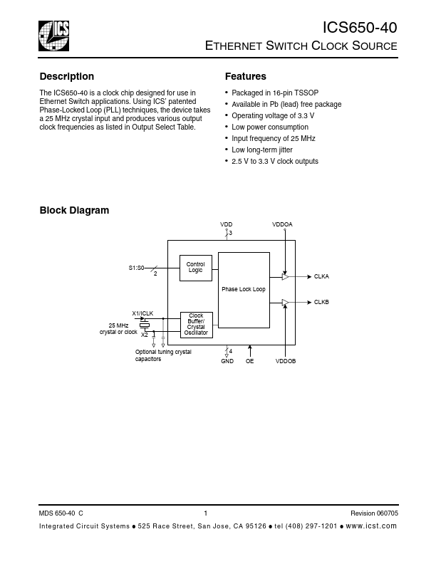
The ICS650-40 is a clock chip designed for use in Ethernet Switch applications.
Using ICS’ patented Phase-Locked Loop (PLL) techniques, the device takes a 25 MHz crystal input and produces various output clock frequencies as listed in Output Select Table.
| Part number | ICS650G-40 |
|---|---|
| Manufacturer | Integrated Circuit Systems |
| File Size | 147.59 KB |
| Description | ETHERNET SWITCH CLOCK SOURCE |
| Datasheet |
ICS650G-40 Datasheet
|
|
|
|
| Part Number | Description | Manufacturer |
|---|---|---|
| ICS650-01 | SYSTEM PERIPHERAL CLOCK SOURCE | Renesas |
| ICS650-07C | NETWORKING CLOCK SOURCE | Renesas |
| ICS650-11 | NETWORKING CLOCK SYNTHESIZER | IDT |
| ICS650-14 | NETWORKING SYSTEM CLOCK | Renesas |
| ICS650-21 | SYSTEM PERIPHERAL CLOCK SOURCE | Renesas |
| Part Number | Description |
|---|---|
| ICS650G-44 | Spread Spectrum Clock Synthesizer |
| ICS650G-36 | Networking & PCI Clock Source |
| ICS650-01B | System Peripheral Clock Source |
| ICS650-05 | HDTV Clock Synthesizer |
| ICS650-07B | Broadcom Clock Source |