Datasheet4U Logo Datasheet4U.com

IS61NVP51218A - 9Mb STATE BUS SRAM

This page provides the datasheet information for the IS61NVP51218A, a member of the IS61NVP25636A 9Mb STATE BUS SRAM family.

Datasheet Summary

Description

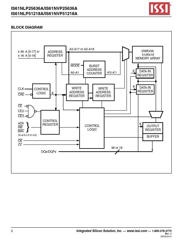
The 9 Meg 'NLP/NVP' product family feature high-speed, low-power synchronous static RAMs designed to provide a burstable, high-performance, 'no wait' state, device for networking and communications applications.

Features

  • 100 percent bus utilization.
  • No wait cycles between Read and Write.
  • Internal self-timed write cycle.
  • Individual Byte Write Control.
  • Single R/W (Read/Write) control pin.
  • Clock controlled, registered address, data and control.
  • Interleaved or linear burst sequence control us- ing MODE input.
  • Three chip enables for simple depth expansion and address pipelining.
  • Power Down mode.
  • Common data inputs and data outp.

📥 Download Datasheet

Datasheet preview – IS61NVP51218A

Datasheet Details

Part number IS61NVP51218A
Manufacturer ISSI
File Size 681.44 KB
Description 9Mb STATE BUS SRAM
Datasheet download datasheet IS61NVP51218A Datasheet
Additional preview pages of the IS61NVP51218A datasheet.
Other Datasheets by ISSI

Full PDF Text Transcription

Click to expand full text
IS61NLP25636A/IS61NVP25636A IS61NLP51218A/IS61NVP51218A  256K x 36 and 512K x 18 9Mb, PIPELINE 'NO WAIT' STATE BUS SRAM AUGUST 2014 FEATURES • 100 percent bus utilization • No wait cycles between Read and Write • Internal self-timed write cycle • Individual Byte Write Control • Single R/W (Read/Write) control pin • Clock controlled, registered address, data and control • Interleaved or linear burst sequence control us- ing MODE input • Three chip enables for simple depth expansion and address pipelining • Power Down mode • Common data inputs and data outputs • CKE pin to enable clock and suspend operation • JEDEC 100-pin TQFP, 165-ball PBGA and 119-ball PBGA packages • Power supply: NVP: Vdd 2.5V (± 5%), Vddq 2.5V (± 5%) NLP: Vdd 3.3V (± 5%), Vddq 3.3V/2.
Published: |