Click to expand full text
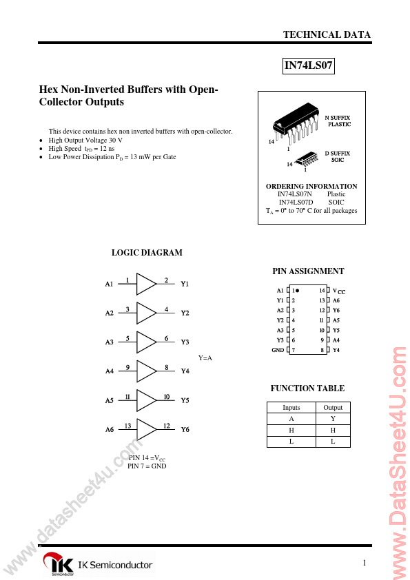
TECHNICAL DATA
IN74LS07 Hex Non-Inverted Buffers with OpenCollector Outputs
This device contains hex non inverted buffers with open-collector. • High Output Voltage 30 V • High Speed tPD = 12 ns • Low Power Dissipation PD = 13 mW per Gate
ORDERING INFORMATION IN74LS07N Plastic IN74LS07D SOIC TA = 0° to 70° C for all packages
LOGIC DIAGRAM PIN ASSIGNMENT
Y=A
FUNCTION TABLE
Inputs A H L Output Y H L
w
w
w
.d
e e h s a t a
. u t4
m o c
PIN 14 =VCC PIN 7 = GND
1
www.DataSheet4U.com
IN74LS07
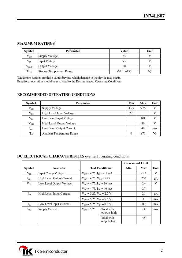
MAXIMUM RATINGS*
Symbol VCC VIN VOUT Tstg
*
Parameter Supply Voltage Input Voltage Output Voltage Storage Temperature Range
Value 7.0 5.5 30 -65 to +150
Unit V V V °C
Maximum Ratings are those values beyond which damage to the device may occur.
 IN74LS07 Datasheet