Datasheet4U Logo Datasheet4U.com

9LPRS501 - ICS9LPRS501

Description

3.3V PCI clock output or Clock Request control A for either SRC0 or SRC2 pair The power-up default is PCI0 output, but this pin may also be used as a Clock Request control of SRC pair 0 or SRC pair 2 via SMBus.

Features

  • es/Benefits: Does not require external pass transistor for voltage regulator Integrated series resistors on differential outputs, Zo=50Ω Supports spread spectrum modulation, default is 0.5% down spread Uses external 14.318MHz crystal, external crystal load caps are required for frequency tuning One differential push-pull pair selectable between SRC and two single-ended outputs Table 1: CPU Frequency Select Table FSLC B0b7 0 0 0 0 1 1 1 1 2 TSSOP Pin Configuration USB MHz DOT MHz FSLB B0b6 0 0.

📥 Download Datasheet

Datasheet Details

Part number 9LPRS501
Manufacturer IDT
File Size 244.67 KB
Description ICS9LPRS501
Datasheet download datasheet 9LPRS501 Datasheet

Full PDF Text Transcription

Click to expand full text
Datasheet 64-PIN CK505 W/FULLY INTEGRATED VOLTAGE REGULATOR + INTEGRATED SERIES RESISTOR Recommended Application: CK505 compliant clock with fully integrated voltage regulator and Internal series resistor on differential outputs, PCIe Gen 1 compliant ICS9LPRS501 Key Specifications: • • • • CPU outputs cycle-cycle jitter < 85ps SRC output cycle-cycle jitter < 125ps PCI outputs cycle-cycle jitter < 250ps +/- 100ppm frequency accuracy on CPU & SRC clocks Output Features: 
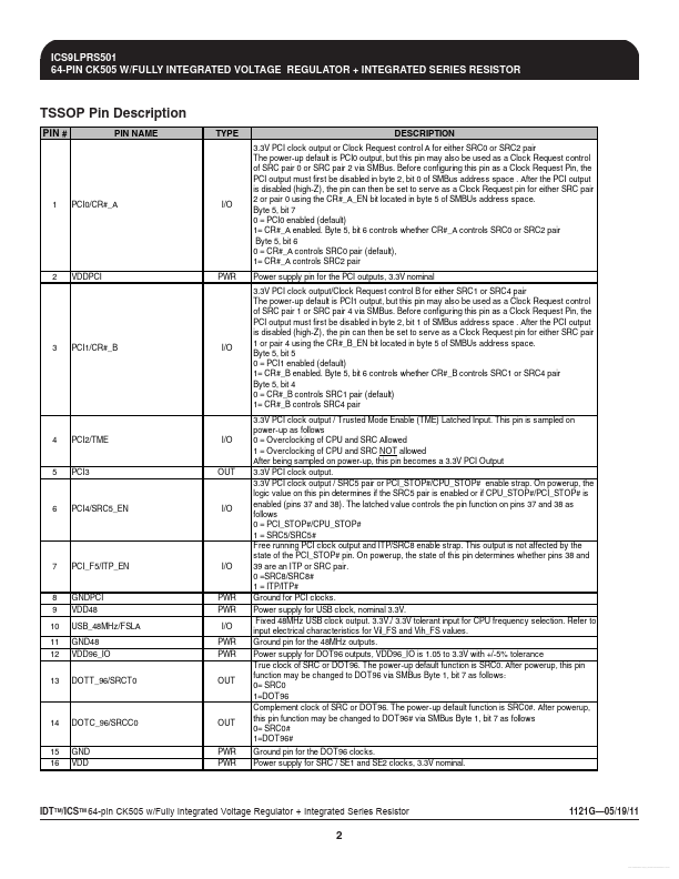
• • • • • • • • 2 - CPU differential low power push-pull pairs 10 - SRC differential low power push-pull pairs 1 - CPU/SRC selectable differential low power push-pull pair 1 - SRC/DOT selectable differential low power push-pull pair 5 - PCI, 33MHz 1 - PCI_F, 33MHz free running 1 - USB, 48MHz 1 - REF, 14.
Published: |