Datasheet Details
| Part number | 9DBL0455 |
|---|---|
| Manufacturer | IDT |
| File Size | 304.09 KB |
| Description | PCIe Gen1-5 Clock Fanout Buffers |
| Datasheet |
 9DBL0455 Datasheet 9DBL0455 Datasheet
|
|
|
Download the 9DBL0455 datasheet PDF. This datasheet also includes the 9DBL0255 variant, as both parts are published together in a single manufacturer document.
| Part number | 9DBL0455 |
|---|---|
| Manufacturer | IDT |
| File Size | 304.09 KB |
| Description | PCIe Gen1-5 Clock Fanout Buffers |
| Datasheet |
9DBL0455 Datasheet
|
|
|
|
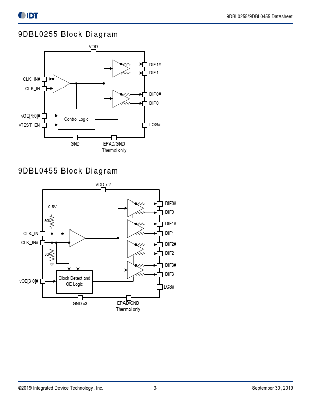
The 9DBL0255/9DBL0455 are 2 and 4-output PCIe clock fanout buffers for PCIe Gen1–5 applications.
Both parts have a open drain Loss of Signal (LOS) output to indicate the absence or presence of an input clock.
The devices implement several additional
2 and 4-Output 3.3V PCIe Gen1–5 Clock Fanout Buffers with LOS.
| Brand Logo | Part Number | Description | Manufacturer |
|---|---|---|---|
| 9DBL0455 | 2 and 4-Output 3.3V PCIe Gen1-5 Clock Fanout Buffers | Renesas |
| Part Number | Description |
|---|---|
| 9DBL0452 | 4-Output 3.3V PCIe Zero-delay Buffer |
| 9DBL0453 | 4-output 3.3V LP-HCSL Zero-Delay Buffer |
| 9DBL04 | 4-output 3.3V PCIe Zero-delay Buffer |
| 9DBL0442 | 4-Output 3.3V PCIe Zero-delay Buffer |
| 9DBL0443 | 4-output 3.3V LP-HCSL Zero-Delay Buffer |
| 9DBL02 | 2-output 3.3V PCIe Zero-Delay Buffer |
| 9DBL0242 | 2-output 3.3V PCIe Zero-Delay Buffer |
| 9DBL0243 | 2-Output 3.3V LP-HCSL Zero-Delay Buffer |
| 9DBL0252 | 2-output 3.3V PCIe Zero-Delay Buffer |
| 9DBL0253 | 2-Output 3.3V LP-HCSL Zero-Delay Buffer |