Click to expand full text
Programmable Low Additive Jitter 2:8 Buffer with Dividers and Universal Outputs
8P79818
Datasheet
Description
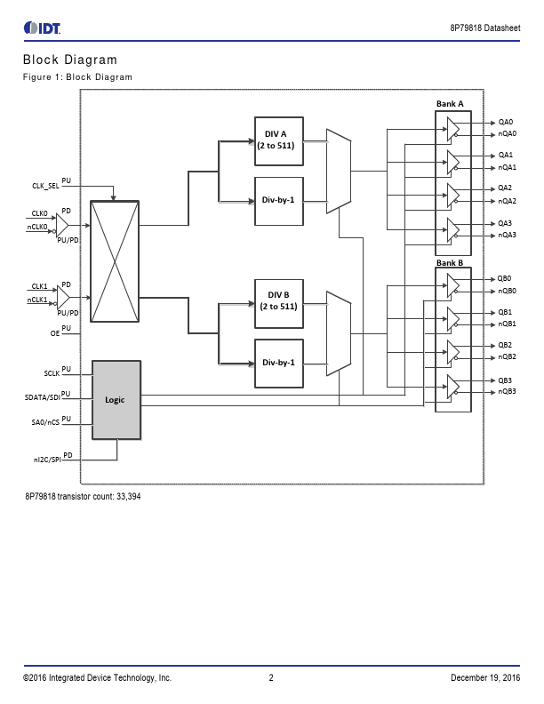
The device is intended to take 1 or 2 reference clocks, select between them, using a pin or register selection and generate up to 8 outputs that may be the same as the reference frequency or integer-divider versions of it.
The 8P79818 supports two output banks, each with its own divider and power supply. All outputs in one bank would generate the same output frequency, but each output can be individually controlled for output type, output enable or even powered-off.
The device supports a serial port for configuration of the parameters while in operation. The serial port can be selected to use the I2C or SPI protocol.
 8P79818 Datasheet