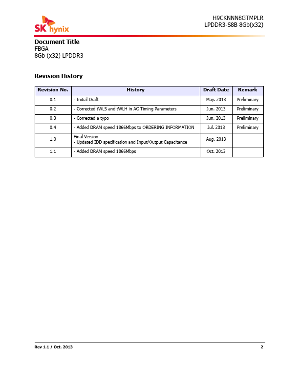
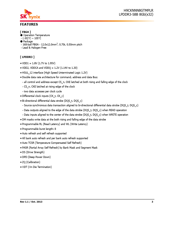
Datasheet4U Logo Datasheet4U.com

H9CKNNN8GTMPLR-NUH - 8Gb LPDDR3

Download the H9CKNNN8GTMPLR-NUH datasheet PDF. This datasheet also covers the H9CKNNN8GTMPLR variant, as both devices belong to the same 8gb lpddr3 family and are provided as variant models within a single manufacturer datasheet.

Description

and is subject to change without notice.

SK hynix does not assume any responsibility for use of circuits described.

No patent licenses are implied.

Features

  • [ FBGA ].
  • Operation Temperature - (-30)oC ~ 105oC.
  • Package - 168-ball FBGA - 12.0x12.0mm2, 0.70t, 0.50mm pitch - Lead & Halogen Free [ LPDDR3 ].
  • VDD1 = 1.8V (1.7V to 1.95V).
  • VDD2, VDDCA and VDDQ = 1.2V (1.14V to 1.30).
  • HSUL_12 interface (High Speed Unterminated Logic 1.2V).
  • Double data rate architecture for command, address and data Bus; - all control and address except CS_n, CKE latched at both rising and falling edge of the clock - CS_n, CKE latched at rising edg.

📥 Download Datasheet

Note: The manufacturer provides a single datasheet file (H9CKNNN8GTMPLR-Hynix.pdf) that lists specifications for multiple related part numbers.

Full PDF Text Transcription

Click to expand full text
168ball FBGA Specification 8Gb LPDDR3 (x32) This document is a general product description and is subject to change without notice. SK hynix does not assume any responsibility for use of circuits described. No patent licenses are implied. Rev 1.1 / Oct. 2013 1 H9CKNNN8GTMPLR LPDDR3-S8B 8Gb(x32) Document Title FBGA 8Gb (x32) LPDDR3 Revision History Revision No. 0.1 0.2 0.3 0.4 1.0 1.1 - Initial Draft - Corrected tWLS and tWLH in AC Timing Parameters - Corrected a typo - Added DRAM speed 1866Mbps to ORDERING INFORMATION Final Version - Updated IDD specification and Input/Output Capacitance - Added DRAM speed 1866Mbps History Draft Date May. 2013 Jun. 2013 Jun. 2013 Jul. 2013 Aug. 2013 Oct. 2013 Remark Preliminary Preliminary Preliminary Preliminary Rev 1.1 / Oct.
Published: |