Click to expand full text
www.DataSheet4U.com
HY5DU56422D(L)TP HY5DU56822D(L)TP HY5DU561622D(L)TP
256M DDR SDRAM
HY5DU56422D(L)TP HY5DU56822D(L)TP HY5DU561622D(L)TP
This document is a general product description and is subject to change without notice. Hynix semiconductor does not assume any responsibility for use of circuits described. No patent licenses are implied. Rev. 0.1 /May 2004
www.DataSheet4U.com
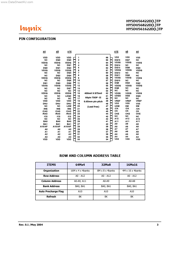
HY5DU56422D(L)TP HY5DU56822D(L)TP HY5DU561622D(L)TP DESCRIPTION
PRELIMINARY
The Hynix HY5DU56422D(L)TP, HY5DU56822D(L)TP and HY5DU561622(L)TP are a 268,435,456-bit CMOS Double Data Rate(DDR) Synchronous DRAM, ideally suited for the main memory applications which requires large memory density and high bandwidth.
 HY5DU56422DTP Datasheet