Click to expand full text
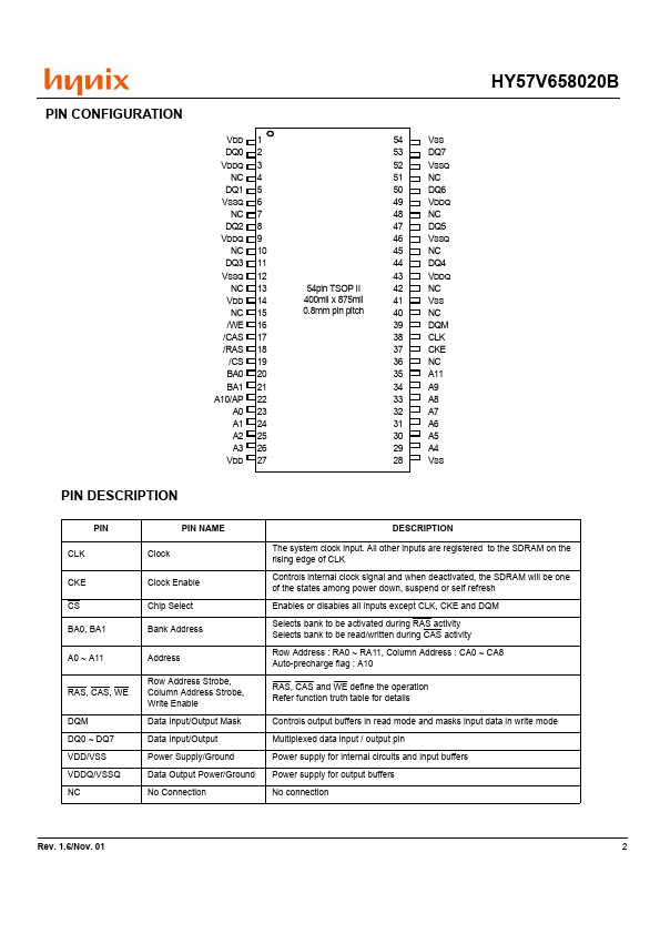
HY57V658020B
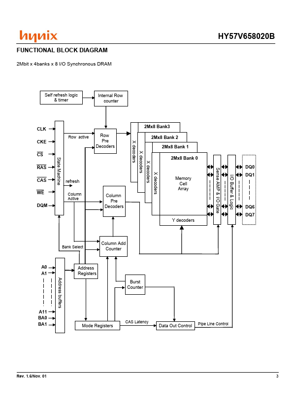
4 Banks x 2M x 8Bit Synchronous DRAM
DESCRIPTION
The Hynix HY57V658020B is a 67,108,864-bit CMOS Synchronous DRAM, ideally suited for the main memory applications which require large memory density and high bandwidth. HY57V658020B is organized as 4banks of 2,097,152x8. HY57V658020B is offering fully synchronous operation referenced to a positive edge of the clock. All inputs and outputs are synchronized with the rising edge of the clock input. The data paths are internally pipelined to achieve very high bandwidth. All input and output voltage levels are compatible with LVTTL.
 HY57V658020B Datasheet