Click to expand full text
HY57V651620B
4 Banks x 1M x 16Bit Synchronous DRAM
DESCRIPTION
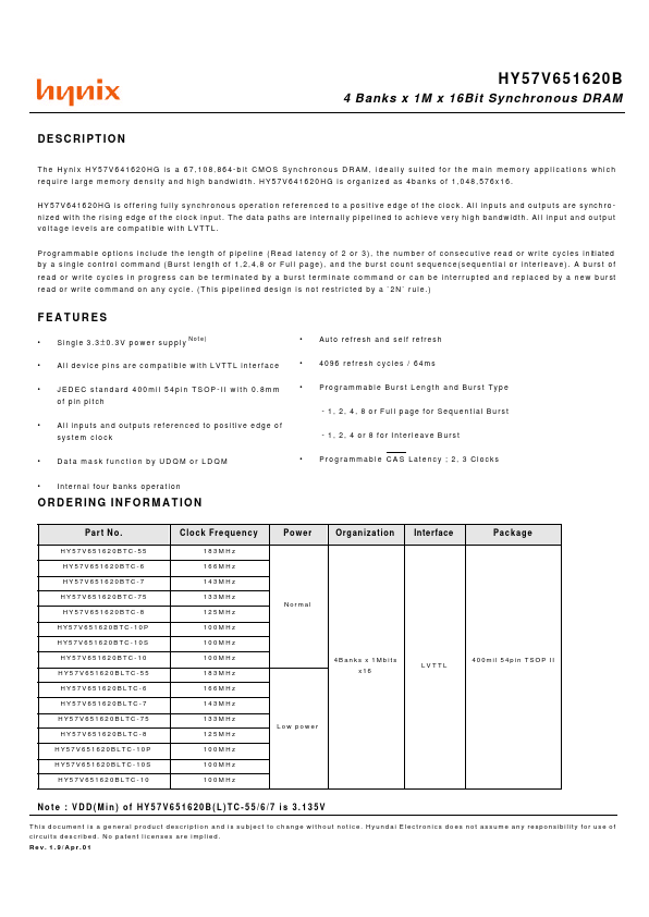
The Hynix HY57V641620HG is a 67,108,864-bit CMOS Synchronous DRAM, ideally suited for the main memory applications which require large memory density and high bandwidth. HY57V641620HG is organized as 4banks of 1,048,576x16. H Y 5 7 V 6 4 1 6 2 0 H G i s o f f e r i n g f u l l y s y n c h r o n o u s o p e r a t i o n r e f e r e n c e d t o a p o s i t i v e e d g e o f t h e c l o c k . A l l i n p u t s a n d o u t p u t s a r e s y nc h r o nized with the rising edge of the clock input. The data paths are internally pipelined to achieve very high bandwidth. All input and output voltage levels are compatible with LVTTL.
 HY57V651620B Datasheet