Suitable for switching regulator and DC-DC converter
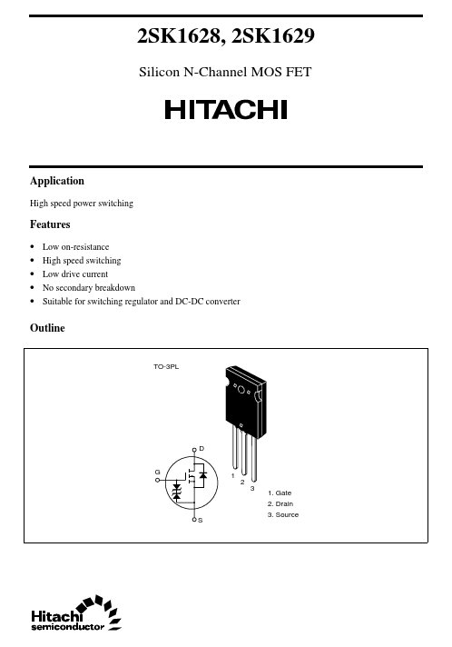
Outline
TO-220FM
D 12 3 1. Gate
G 2. Drain 3. Source
S
2SK1626, 2SK1627
Absolute Maximum Ratings (Ta = 25°C)
Item
Drain to source voltage
2SK1626
2SK1627
Gate to source voltage
Drain current
Drain peak current
Body to drain diode reverse drain current
Channel dissipation
Channel temperature
Storage temp.
Note: Below is a high-fidelity text extraction (approx. 800 characters) for
K1626. For precise diagrams, and layout, please refer to the original PDF.
2SK1626, 2SK1627 Silicon N-Channel MOS FET Application High speed power switching Features • Low on-resistance • High speed switching • Low drive current • No secondary b...
View more extracted text
resistance • High speed switching • Low drive current • No secondary breakdown • Suitable for switching regulator and DC-DC converter Outline TO-220FM D 12 3 1. Gate G 2. Drain 3. Source S 2SK1626, 2SK1627 Absolute Maximum Ratings (Ta = 25°C) Item Drain to source voltage 2SK1626 2SK1627 Gate to source voltage Drain current Drain peak current Body to drain diode reverse drain current Channel dissipation Channel temperature Storage temperature Note 1. PW ≤ 10 µs, duty cycle ≤ 1% 2.
More Datasheets from Hitachi Semiconductor (now Renesas)
 K1626 Datasheet