Click to expand full text
HD74HCT374/HD74HCT534
Octal D-type Flip-Flops (with 3-state outputs)/ Octal D-type Flip-Flops (with inverted 3-state outputs)
Description
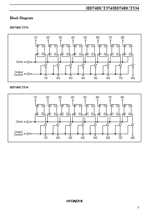
These device are positive edge triggered flip-flops. The difference between HD74HCT374 and HD74HCT534 is only that the former is a true outputs and the latter is a false outputs. Data at the D inputs, meeting the setup and hold time requirements, are transferred to the Q outputs on positive going transitions of the clock (CK) input. When a high logic level is applied to the output control (OC) input, all outputs go to a high impedance state, regardless of what signals are present at the other inputs and the state of the storage elements.
 HD74HCT534 Datasheet