Click to expand full text
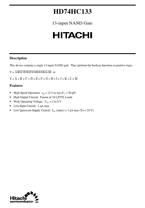
HD74HC133
13-input NAND Gate
Description
This device contains a single 13-input NAND gate. They perform the boolean functions in positive logic. Y = A•B•C•D•E•F•G•H•I•J•K•L•M or Y=A+B + C + D+E+ F + G+H+I+ J+ K+L+ M
Features
• • • • • High Speed Operation: tpd = 12.5 ns typ (CL = 50 pF) High Output Current: Fanout of 10 LSTTL Loads Wide Operating Voltage: VCC = 2 to 6 V Low Input Current: 1 µA max Low Quiescent Supply Current: ICC (static) = 1 µA max (Ta = 25°C)
HD74HC133
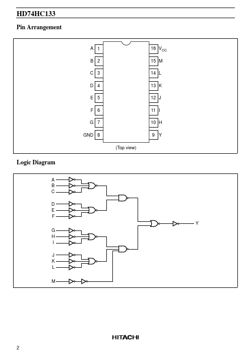
Pin Arrangement
A 1 B 2 C 3 D 4 E 5 F 6 G 7 GND 8 (Top view)
16 VCC 15 M 14 L 13 K 12 J 11 I 10 H 9 Y
Logic Diagram
A B C D E F Y G H I J K L M
2
HD74HC133
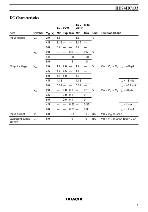
DC Characteristics
Ta = 25°C Item Input voltage Symbol VIH Ta = –40 to +85°C Max — — — 0.5 1.35 1.8 — — — — — 0.1 0.1 0.1 0.33 0.33 ±1.
 HD74HC133 Datasheet