Datasheet Details
| Part number | HD74AC166 |
|---|---|
| Manufacturer | Hitachi Semiconductor (now Renesas) |
| File Size | 65.71 KB |
| Description | 8-bit Shift Register |
| Datasheet |
 HD74AC166 Datasheet HD74AC166 Datasheet
|
|
|
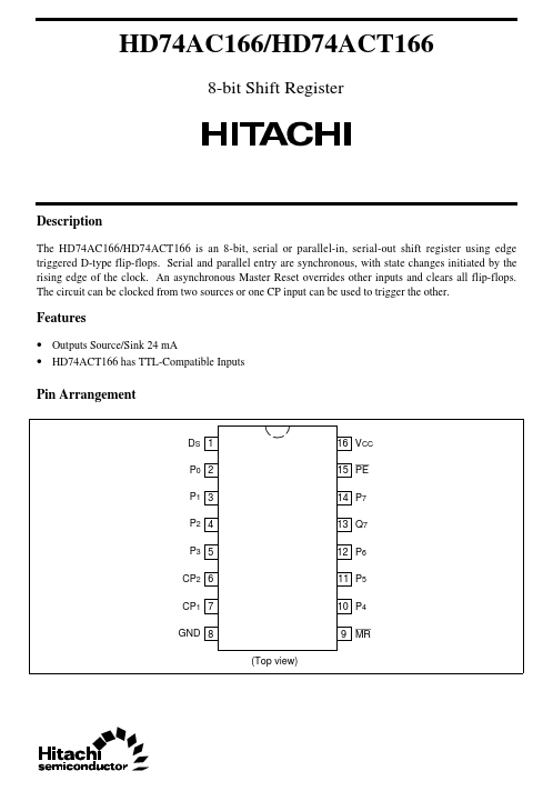
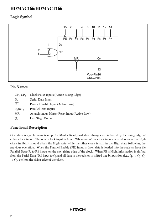
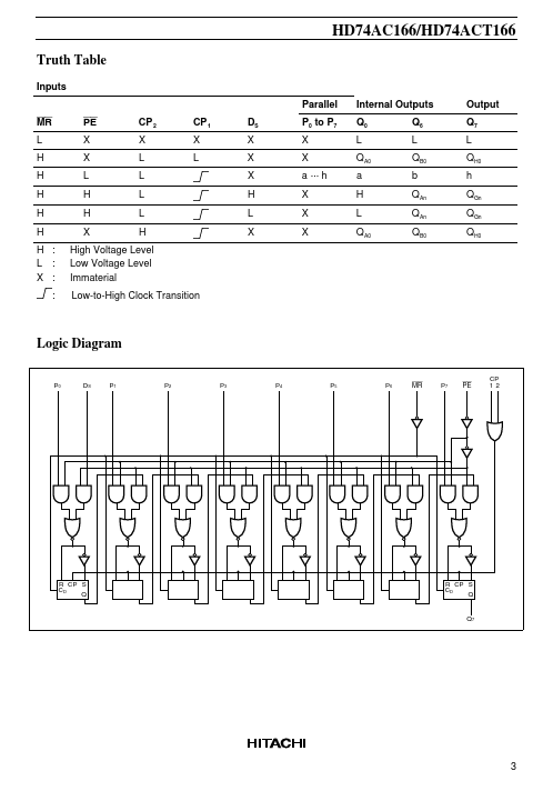
The HD74AC166/HD74ACT166 is an 8-bit, serial or parallel-in, serial-out shift register using edge triggered D-type flip-flops.
Serial and parallel entry are synchronous, with state changes initiated by the rising edge of the clock.
| Part number | HD74AC166 |
|---|---|
| Manufacturer | Hitachi Semiconductor (now Renesas) |
| File Size | 65.71 KB |
| Description | 8-bit Shift Register |
| Datasheet |
HD74AC166 Datasheet
|
|
|
|
| Part Number | Description | Manufacturer |
|---|---|---|
| HD74AC166 | 8-bit Shift Register | Renesas |
| HD74AC164 | Shift Register | Renesas |
| HD74AC165 | Parallel-Load 8-bit Shift Register | Renesas |
| HD74AC107 | Dual JK Flip-Flop | Renesas |
| HD74AC112 | Dual JK Negative Edge-Triggered Flip-Flop | Renesas |
| Part Number | Description |
|---|---|
| HD74AC164 | Serial-In/ Parallel-Out Shift Register |
| HD74AC165 | Parallel-Load 8-bit Shift Register |
| HD74AC107 | Dual JK Flip-Flop (with Separate Clear and Clock) |
| HD74AC112 | Dual JK Negative Edge-Triggered Flip-Flop |
| HD74AC123A | Dual Retriggerable Resettable Multivibrator |